Rf02 – Rainbow Electronics RF02 User Manual
Page 8
RF02
Tel: +86-755-86096587 Fax: +86-755-86096602 E-mail: [email protected] http://www.hoperf.com
C
o
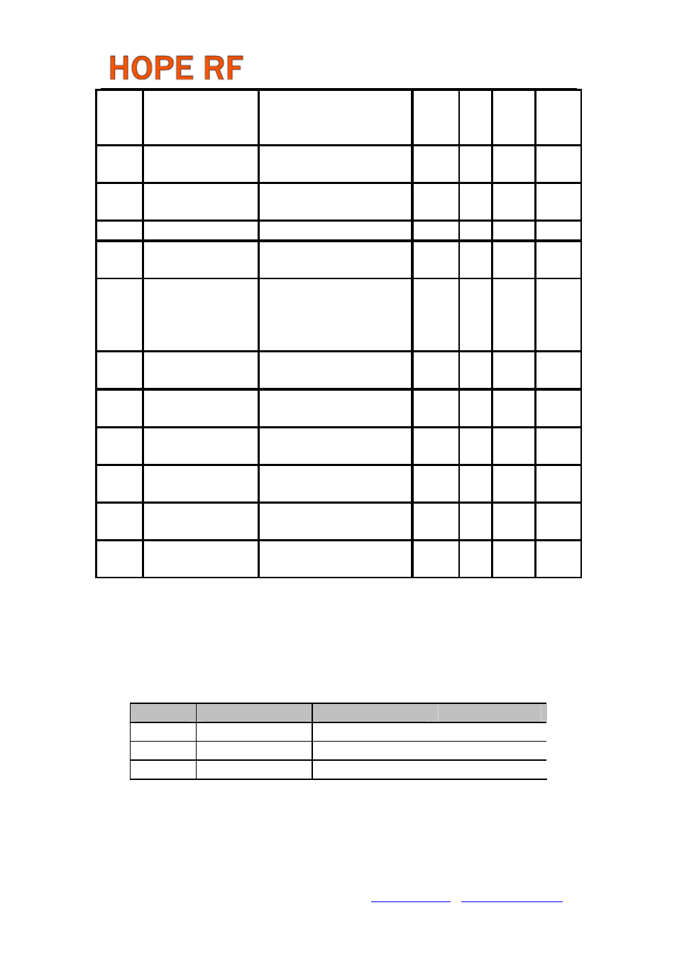
Output capacitance
(set by the automatic
antenna tuning circuit)
At low bands
At high bands
1.5
1.6
2.3
2.2
2.8
3.1 pF
Q
o
Quality factor of the
output capacitance
16
18
22
pF
L
out
Output phase noise
100 kHz from carrier
1 MHz from carrier (Note 7)
-85
-105
dBc/Hz
BR
FSK
FSK bit rate
(Note 7)
115.2
kbps
df
fsk
FSK frequency
deviation
Programmable in 30 kHz steps
30 210
kHz
C
xl
Crystal load
capacitance See
Crystal Selection
Guidelines
Programmable in 0.5 pF steps,
tolerance +/-10%
8.5 16
pF
t
POR
Internal POR timeout
(Note 6)
After V
dd
has reached 90% of
final value
50
ms
t
sx
Crystal oscillator
startup time
Crystal ESR < 100 Ohms
1.5 5
ms
t
PBt
Wake-up timer clock
period
Calibrated every 30 seconds
0.95 1.05
ms
t
wake-up
Programmable
wake-up time
1
5
*10
11
ms
C
in, D
Digital input
capacitance
2
pF
t
r, f
Digital output rise/fall
time
15 pF pure capacitive load
10
ns
Note 1:
Using a CR2032 battery (225 mAh capacity), the expected battery life is greater than 2 years
using a 60-second wake-up period for sending 50 byte packets in length at 19.2 kbps with +6 dBm output
power in the 915 MHz band.
Note 2:
Using anything but a 10 MHz crystal is allowed but not recommended because all
crystal-referred timing and frequency parameters will change accordingly.
Note 3:
Adjustable in 8 steps.
Note 4:
Optimal antenna admittance/impedance for the RF02:
Yantenna [S]
Zantenna [Ohm]
Lantenna [nH]
434 MHz
1.3E-3 - j6.3E-3
31 + j152
58.00
868 MHz
1.35E-3 - j1.2E-2
9 + j82
15.20
915 MHz
1.45E-3 - j1.3E-2
8.7 + j77
13.60
Note 5:
With selective resonant antennas .
Note 6:
During this period, no commands are accepted by the chip.
Note 7:
The maximum FSK bitrate and the Output phase noise are dependent on the actual setting of the
PLL Setting Command.