U3742bm – Rainbow Electronics U3742BM User Manual
Page 17
17
U3742BM
4735A–RKE–11/03
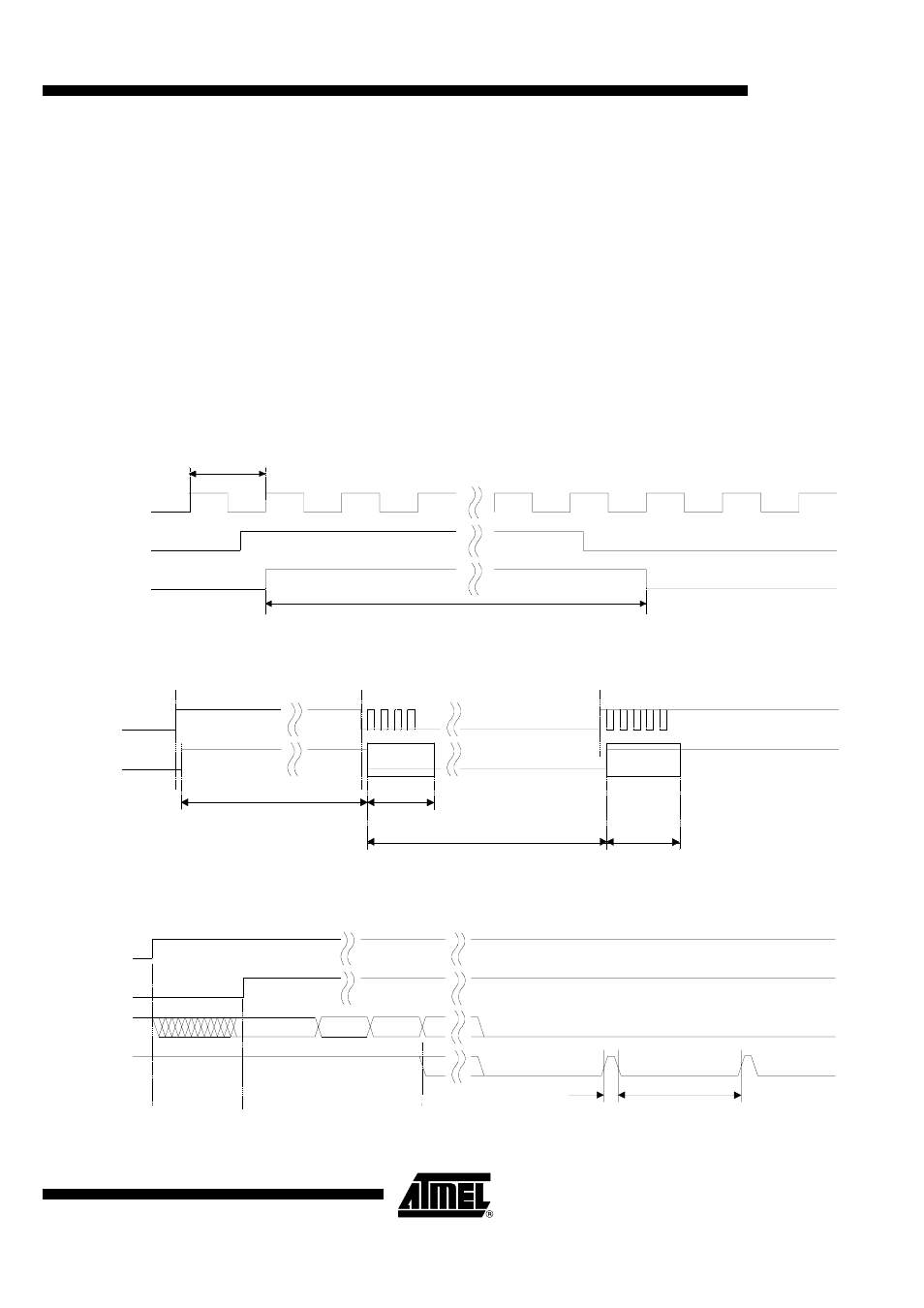
The minimum time period between two edges of the data signal is limited to
t
ee
³
T
DATA_min
. This implies an efficient suppression of spikes at the DATA output. At the
same time, it limits the maximum frequency of edges at DATA. This eases the interrupt
handling of a connected microcontroller. T
DATA_min
is to some extent affected by the pre-
ceding edge-to-edge time interval tee as illustrated in Figure 19. If t
ee
is in between the
s p e c i fi e d b i t c h e c k l i m i ts , t he f o l l ow i n g l e v e l i s f ro z e n f o r th e t i me p e ri o d
T
DATA_min
= tmin1, in case of t
ee
being outside that bit check limits T
DATA_min
= tmin2 is
the relevant stable time period.
The maximum time period for DATA to be Low is limited to T
DATA_L_max
. This function
ensures a finite response time during programming or switching off the receiver via pin
DATA. T
DATA_L_max
is thereby longer than the maximum time period indicated by the
transmitter data stream. Figure 20 gives an example where Dem_out remains Low after
the receiver is in receiving mode.
Figure 18. Synchronization of the Demodulator Output
Figure 19. Debouncing of the Demodulator Output
Figure 20. Steady L State Limited DATA Output Pattern after Transmission
Clock bit check
Counter
DATA
T
XClk
Dem_out
t
ee
DATA
tmin1
CV_Lim < Lim_min or CV_Lim
≥
Lim_max
Lim_min
≤
CV_Lim < Lim_max
Dem_out
t
ee
t
ee
tmin2
Bit check
Enable IC
DATA
Startup mode
Receiving mode
tmin2
Bit check mode
t
DATA_L_max
Dem_out