U3742bm – Rainbow Electronics U3742BM User Manual
Page 14
14
U3742BM
4735A–RKE–11/03
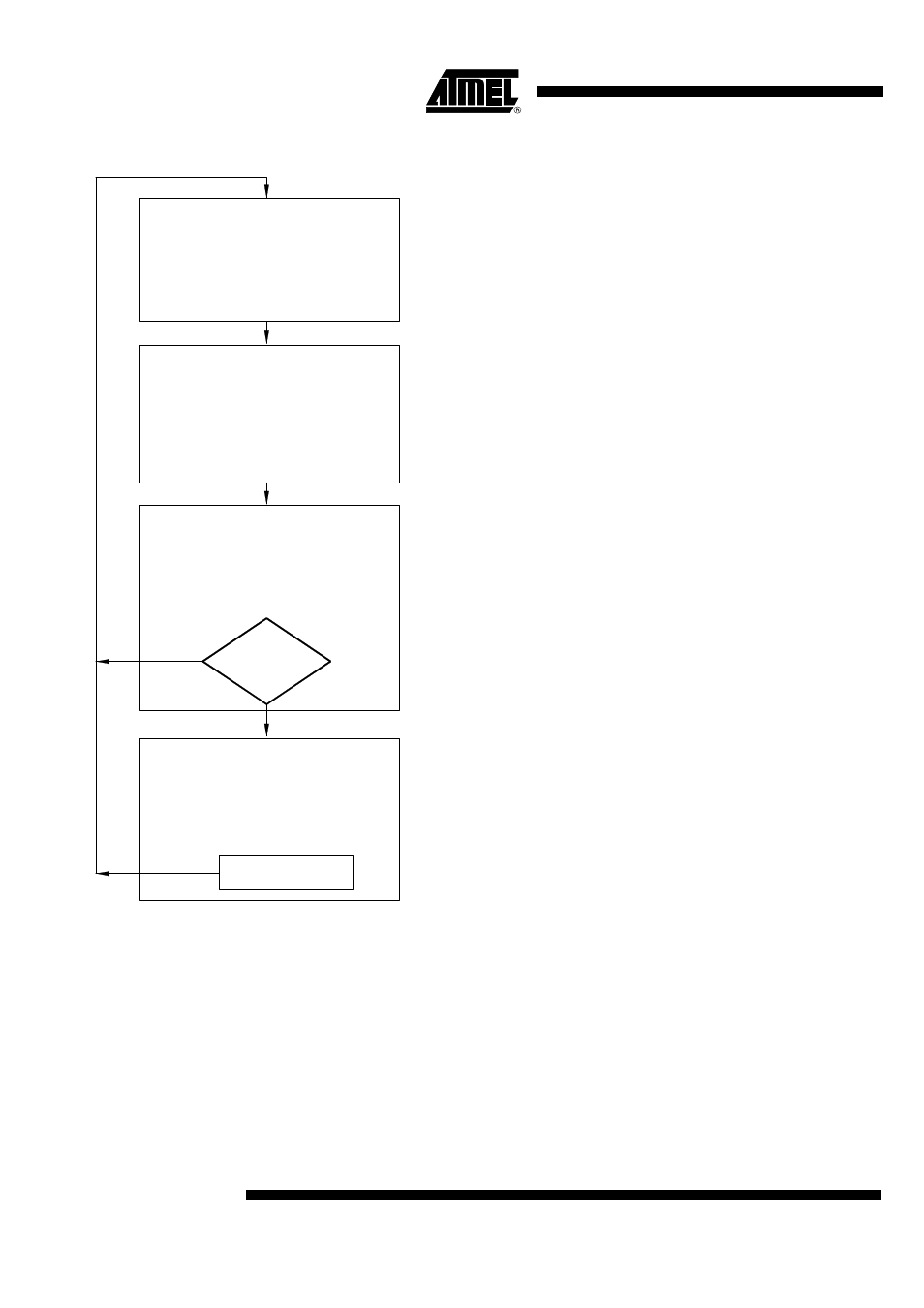
Figure 13. Polling Mode Flow Chart
Sleep mode:
All circuits for signal processing
are disabled. Only XTO and
polling logic are enabled.
I
S
= I
Soff
T
Sleep
= Sleep
×
X
Sleep
Ч
1024
Ч
T
Clk
Start-up mode:
The signal processing circuits are
enabled. After the start-up time
(T
Startup
) all circuits are in stable
condition and ready to receive.
I
S
= I
Son
T
Startup
Bit check mode:
The incoming data stream is
analyzed. If the timing indicates a
valid transmitter signal, the receiver
is set to receiving mode. Otherwise
it is set to Sleep mode.
T
Bitcheck
Receiving mode:
The receiver is turned on permanently
and passes the data stream to the
connected microcontroller. It can be set
to Sleep mode through an OFF
command via pin DATA or ENABLE.
Bit check
OK ?
OFF command
Sleep: 5-bit word defined by Sleep0 to
Sleep4 in OPMODE register
X
Sleep
: Extension factor defined by
XSleep
Std
and XSleep
Temp
according to Table 8
T
CLK
: Basic clock cycle defined by f
XTO
and pin MODE
T
Startup
: Is defined by the selected baud rate range and T
Clk
.
The baud rate range is defined by Baud0 and Baud1
in the OPMODE register.
T
Bitcheck
: Depends on the result of the bit check
If the bit check is ok, T
bitcheck
depends on
the number of bits to be checked (N
Bitcheck
)
and on the utilized data rate.
If the bit check fails, the average time period for
that check depends on the selected baud rate
range and on T
Clk
. The baud rate is defined by
Baud0 and Baud1 in the OPMODE register.
NO
YES
I
S
= I
Son
I
S
= I
Son