U3742bm, Receiving mode – Rainbow Electronics U3742BM User Manual
Page 16
16
U3742BM
4735A–RKE–11/03
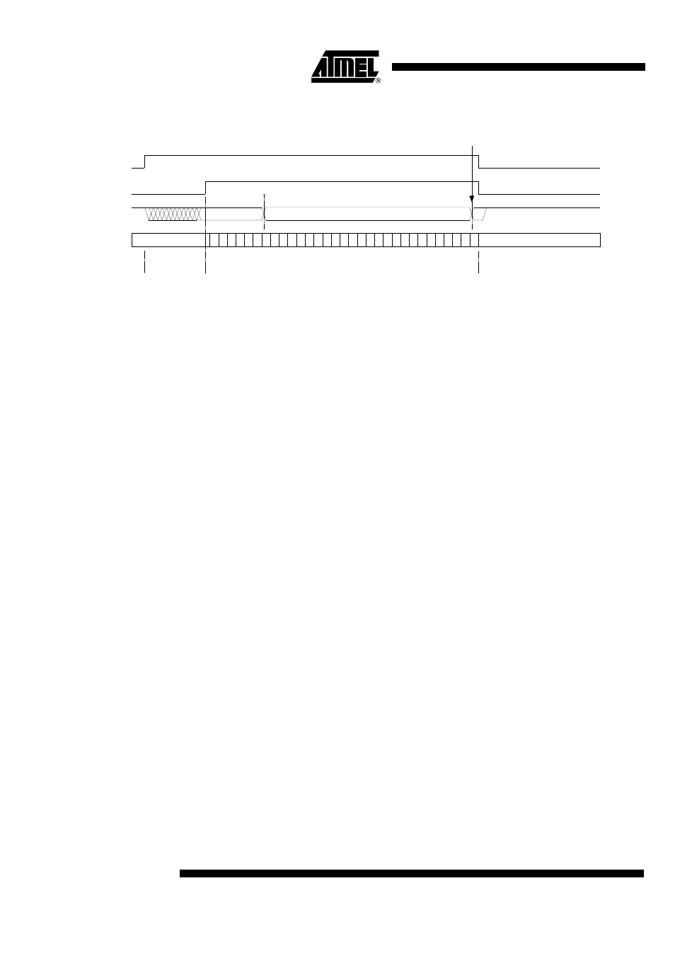
Figure 17. Timing Diagram for Failed Bit Check (Condition: CV_Lim
³
Lim_max)
Figure 15 to Figure 17 illustrate the bit check for the default bit check limits
Lim_min = 14 and Lim_max = 24. When the IC is enabled, the signal processing circuits
are enabled during T
Startup
. The output of the ASK/FSK demodulator (Dem_out) is unde-
fined during that period. When the bit check becomes active, the bit check counter is
clocked with the cycle T
XClk
.
Figure 15 on page 15 shows how the bit check proceeds if the bit check counter value
CV_Lim is within the limits defined by Lim_min and Lim_max at the occurrence of a sig-
nal edge. In Figure 16 on page 15, the bit check fails as the value CV_lim is lower than
the limit Lim_min. The bit check also fails if CV_Lim reaches Lim_max. This is illustrated
in Figure 17.
Duration of the Bit Check
If no transmitter signal is present during the bit check, the output of the ASK/FSK
demodulator delivers random signals. The bit check is a statistical process and T
Bitcheck
varies for each check. Therefore, an average value for T
Bitcheck
is given in the electrical
characteristics. T
Bitcheck
depends on the selected baud rate range and on T
Clk
. A higher
baud rate range causes a lower value for T
Bitcheck
resulting in a lower current consump-
tion in polling mode.
In the presence of a valid transmitter signal, T
Bitcheck
is dependant on the frequency of
that signal, f
Sig
and the count of the checked bits, N
Bitcheck
. A higher value for N
Bitcheck
thereby results in a longer period for T
Bitcheck
requiring a higher value for the transmitter
preburst T
Preburst
.
Receiving Mode
If the bit check has been successful for all bits specified by N
Bitcheck
, the receiver
switches to receiving mode. According to Figure 14, the internal data signal is switched
to pin DATA in that case. A connected microcontroller can be woken up by the negative
edge at pin DATA. The receiver stays in that condition until it is switched back to polling
mode explicitly.
Digital Signal Processing
The data from the ASK/FSK demodulator (Dem_out) is digitally processed in different
ways and as a result converted into the output signal data. This processing depends on
the selected baud rate range (BR_Range). Figure 18 on page 17 illustrates how
Dem_out is synchronized by the extended clock cycle T
XClk
. This clock is also used for
the bit check counter. Data can change its state only after T
XClk
elapsed. The
edge-to-edge time period t
ee
of the Data signal as a result is always an integral multiple
of T
XClk
.
Bit check
Enable IC
Bit check counter
0
2 3 4 5 6
2
4 5
1
7
3
6 7 8 9
1112
10
1/2 Bit
Startup mode
20
(Lim_min = 14, Lim_max = 24)
Sleep mode
Bit check failed (CV_Lim
≥
Lim_max)
13141516171819
21222324
0
1
Dem_out
Bit check mode