Rainbow Electronics MAX9476 User Manual
Page 2
MAX9476
Low-Jitter, 8kHz Reference
Clock Synthesizer Outputs 35.328MHz
2
_______________________________________________________________________________________
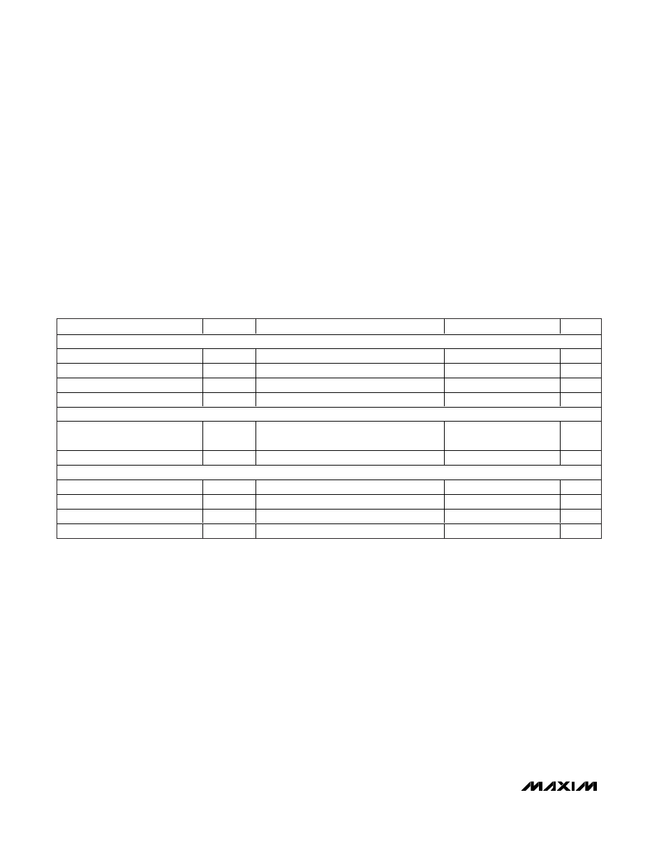
ABSOLUTE MAXIMUM RATINGS
DC ELECTRICAL CHARACTERISTICS
(V
DD
= V
DDP
= +3.0V to +3.6V, T
A
= -40°C to +85°C, unless otherwise noted. Typical values are at V
DD
= V
DDP
= +3.3V, T
A
=
+25
°C.) (Note 1)
Stresses beyond those listed under “Absolute Maximum Ratings” may cause permanent damage to the device. These are stress ratings only, and functional
operation of the device at these or any other conditions beyond those indicated in the operational sections of the specifications is not implied. Exposure to
absolute maximum rating conditions for extended periods may affect device reliability.
V
DD
to GND ...........................................................-0.3V to +4.0V
V
DDP
to GNDP.......................................................-0.3V to +4.0V
SHDN, REO, REIN, X1, X2, CLK_ to GND ...-0.3V to (V
DD
+ 0.3V)
LP1, SETI to GNDP.....................................-0.3V to (V
DD
+ 0.3V)
LP2 Internally Connected to GNDP
Short-Circuit Duration of Outputs ...............................Continuous
Continuous Power Dissipation (T
A
= +70°C)
24-Pin TSSOP (derate 12.2mW/°C above +70°C) .......976mW
Operating Temperature Range ...........................-40°C to +85°C
Maximum Junction Temperature .....................................+150°C
Storage Temperature Range .............................-60°C to +150°C
ESD Rating (Human Body Model) .......................................±2kV
Lead Temperature (soldering, 10s) .................................+300°C
PARAMETER
SYMBOL
CONDITIONS
MIN
TYP
MAX
UNITS
DIGITAL INPUTS (REIN,
SHDN)
Input-High Logic Level
V
IH
2.0
V
Input-Low Logic Level
V
IL
0.8
V
Input-Current High Level
I
IH
V
IN
= V
DD
20
µA
Input-Current Low Level
I
IL
V
IN
= 0
-20
µA
DIGITAL OUTPUT CLOCKS (CLK1–CLK6, REO)
Output-High Logic Level
V
OH
I
OH
= -4mA
V
DD
-
0.6V
V
Output-Low Logic Level
V
OL
I
OL
= 4mA
0.4
V
POWER SUPPLY (V
DD
, V
DDP
)
Power-Supply Range
V
DD
3.0
3.6
V
PLL Power-Supply Range
V
DDP
3.0
3.6
V
Power-Supply Current
I
DD
+ I
DDP
(Note 2)
9
16
mA
Shutdown Supply Current
I
SHDN
7.5
30
µA