Toshiba TLP511E User Manual
Page 9
4-2
1
2
3
4
5
6
7
8
9 10 11 12 Pixel
Inverted phase 2
voltage
Inverted phase 1
voltage
Center voltage
1st line
2nd line
1
2
3
4
5
6
7
8
9 10 11 12
Pixel
Normal phase 1
voltage
Normal phase 2
voltage
Inverted phase
2 voltage
Inverted phase
1 voltage
2nd line
1
2
3
1 2
3
4
5 6
7
8 9 10 11 12 Pixel
4
5
6
7
8
9
10 11 12
Pixel
Center voltage
1st line
Normal phase 1
voltage
Normal phase 2
voltage
The signal as shown in Fig. 4-1-1 is separated into the
odd and even pixels at the digital PC board. After the
signal process is carried out in the drive PC board, the
odd and even pixel signals are synthesized to
decomposite the signal on the panel.
Referring to Fig. 4-1-1, the operation principle is
described.
When assuming;
1) the signal passing through DAC1
®
Q502
®
Normal
amp. 1
®
SW31
®
SW5
®
Q516 to the positive
phase 1,
2) the signal passing through DAC1
®
Q502
®
inverted
amp. 1
®
SW32
®
SW5
®
Q516 to the inverted
phase 1,
3) the signal passing through DAC2
®
Q504
®
Normal
amp. 1
®
SW41
®
SW6
®
Q517 to the positive
phase 2 and
4) the signal passing through DAC2
®
Q504
®
inverted
amp. 2
®
SW42
®
SW6
®
Q517 to inverted phase
2,
the AC and DC levels of the positive phases 1, 2 and the
inverted phases 1, 2 are expected to be the same.
However, each voltage will vary slightly owing to the
adjustment variation. In this case, each frame signal is
assumed as follows.
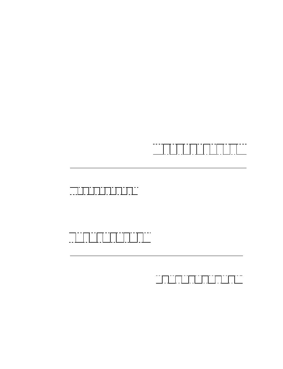
<1st frame>
<2nd line>
Fig. 4-1-4
As shown in Fig. 4-1-4, even if a slight level difference
occurs among the positive phases 1, 2 and inverted
phases 1, 2 signals (approx. 100 mV), the level differ-
ence will be decreased visually by reducing the level
variation of the same line between each frame and
inverting the pixel voltage of the adjacent lines (1st line
and 2nd line) between each frame.