Toshiba TLP511E User Manual
Page 38
7-11
QV001
INPUT SELECTOR
CXA1855Q
VIDEO
RGB
LINEOUT
BUFFER
BUFFER
DAC
VOL / MUTE
SOUND OUT
SPEAKER
1.5W
VOLUME
MUTE
L
R
L
R
L
R
CXA1315M
QA01
M5222FP
QA02
TDA7056A
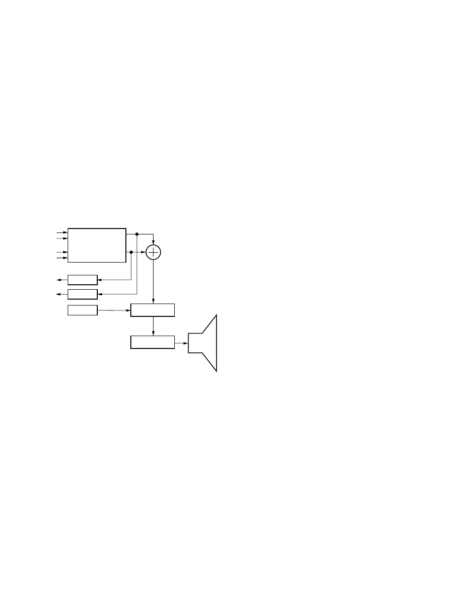
7-3-7. Audio Circuit
Fig. 7-3-12 shows the audio circuit block diagram.
Signal path from the QV001 to the LINE OUT terminal
is: QV001
®
transistor buffer
®
LINE OUT terminal.
Signal path from the QV001 to the speaker is as follows.
The audio signal developed from the QV001 becomes
one signal with its L and R signal components mixed.
The mixed audio signal enters the electrical volume IC
QA01 (M5222FP) and the output level is controlled
within a range of about 0 dB to –80 dB by an external
DC voltage (DAC). The audio signal thus controlled by
the IC QA01 is fed to the speaker amplifier IC QA02
(TDA7056A) and amplified by about 36 dB to drive the
speaker.
Fig. 7-3-12 Audio circuit block diagram