3. video demodulation block -5, 3. video demodulation block – Toshiba TLP511E User Manual
Page 32
7-5
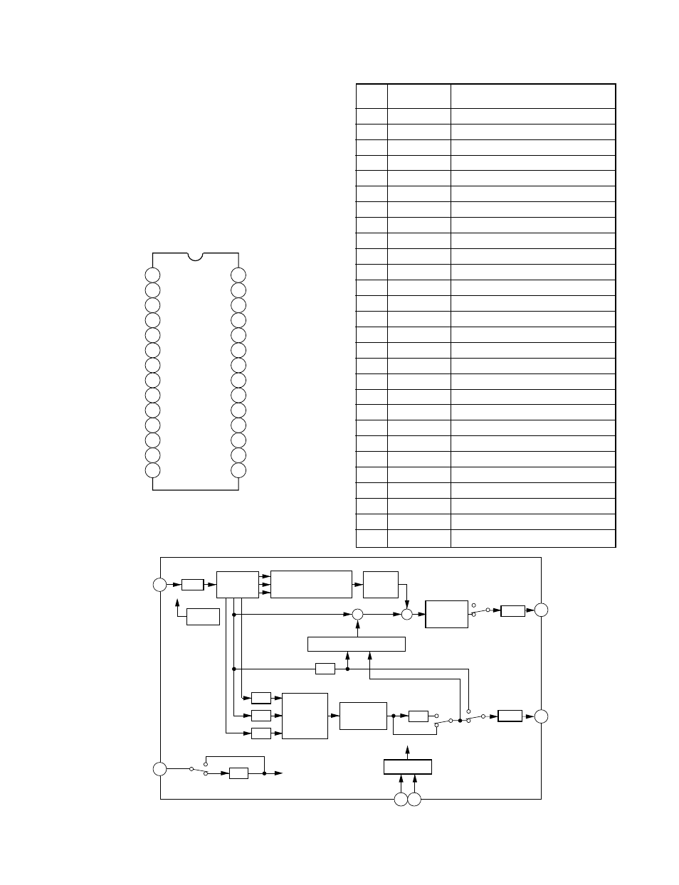
7-3. Video Demodulation Block
7-3-1. Y/C Separation Circuit
This circuit separates Y and C signals from a composite
video signal. Fig. 7-3-1 shows the pin configuration of
TC9090AN and Fig. 7-3-2 shows the block diagram.
The composite video signal enters pin 3. A fsc (3.58/
4.43 MHz) developed from the video/color IC enters pin
19 and is converted into a 4fsc of the drive clock
frequency inside the IC. The composite video signal
entered is processed at a rate of the clock frequency of
the IC and output as Y and C signal.
Fig. 7-3-1 Pin configuration of TC9090AN
Table 7-3-1 Terminal function of TC9090AN
Fig. 7-3-2 Block diagram of TC9090AN
Pin
No.
1
2
3
4
5
6
7
8
9
10
11
12
13
14
15
16
17
18
19
20
21
22
23
24
25
26
27
28
Name
V
REFH
V
SS1
ADIN
V
DD1
V
REFL
BIAS1
P/S
SDA
SCL
RESET
TEST1
TEST2
KILLER
PLLSEL
V
DD3
V
SS3
V
SS2
V
DD2
CKIN
VFIL
2/1 V
DD
BIAS3
C
OUT
BIAS2
Y
OUT
V
REF1
V
DD4
V
SS4
Function
ADC bias
ADC GND
Video input
ADC VDD
ADC bias
ADC bias
Selection function control
I
2
C bus clock input
I
2
C bus data input, check output
I
2
C bus reset
T
est terminal
Test terminal
Clock killer switch
Selection input clock
Digital VDD
Analog GND
PLL GND
PLL VDD
Clock input
VCO filter
Line memory bias
DAC bias
C output
DAC bias
Y output
DAC bias
DAC VDD
DAC GND
2
+
+
25
23
19
8
9
ADC
CLAMP
LINE
MEMORY
VERTICAL EDGE
ENHANCE CIRCUIT
CORING
CIRCUIT
PEDESTAL
CLIP
YDAC
Y
output
C
output
CDAC
8 bits
COLOR KILLER CIRCUIT
BPF
4.43 MHz NTSC
BPF
BPF
BPF
DYNAMIC
COMB
FILTER
1 LINE DOT
IMPROVE
CIRCUIT
BPF
I
2
C BUS
Bus
4 FSC
PLL
Clock
Composite
video signal
8 bits
8 bits
1
2
4
28
27
26
25
3
5
24
6
23
7
22
8
21
9
20
10
19
11
18
12
17
13
16
14
15
V
SS4
V
DD4
V
REF1
Y
OUT
BIAS2
C
OUT
BIAS3
2/1V
DD
VFIL
CKIN
V
DD2
V
SS2
V
SS3
V
DD3
V
REFH
V
SS1
ADIN
V
DD1
V
REFL
BIAS1
P/S
SDA
SCL
RESET
TEST1
TEST2
KILLER
PLLSEL