Toshiba TLP511E User Manual
Page 34
7-7
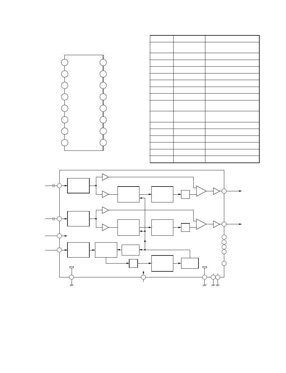
SIGNAL
CLAMPING
SIGNAL
CLAMPING
±
(R-Y)
±
(R-Y)
±
(B-Y)
±
(B-Y)
Color difference
input signals
V
P1
Sand castle
pulse input
analog supply
SANDCASTLE
DETECTOR
GND 1
FREQUENCY
PHASE
DETECTOR
DIVIDER
BY 192
LP
Digital supply
V
P2
GND 2
MED848
DIVIDER
BY 2
6 MHz
CCO
3 MHz shifting clock
LP
SAMPLE
AND
HOLD
LINE
MEMORY
LP
SAMPLE
AND
HOLD
LINE
MEMORY
I.C.
TDA4665
Addition
stages
Output
buffers
Color difference
Output signals
Pre-amplifiers
16
14
9
5
10
1
3
4
7
12
11
8
N.C.
N.C.
N.C.
N.C.
2
6
13
15
TDA9141 has two input terminals for the composite
video/Y signal (pin 25) and C signal (pin 26), and each
of the signals is automatically identified through I
2
C-
BUS control.
Table 7-3-2 Terminal function of TDA4665T
Fig. 7-3-7 Block diagram of TDA4665T
Fig. 7-3-6 Pin configuration of TDA4665T
7-3-3. Luminance (Y) Signal Process Circuit
The processing method differs as follows depending on
type of the signal entered.
(a)
For a SECAM input, it passes through a burst signal
trap circuit.
(b)
For a NTSC/PAL (with burst signal) input (Y/C-sepa-
rated signals), the burst signal trap circuit is bypassed.
It passes through a delay circuit for a phase match-
ing to the color signal.
(c)
For a NTSC/PAL (without burst signal) input, above
trap circuit and the delay circuit are bypassed to per-
form a stable color killer operation.
N.C.
GND1
o(B-Y)
V
o(R-Y)
V
P1
V
GND2
SAND
I.C.
P2
V
N.C.
I.C.
MED849
TDA4665
i(R-Y)
V
N.C.
i(B-Y)
V
1
2
4
3
5
6
7
8
I.C.
N.C.
16
15
13
14
12
11
10
9
Pin No.
1
2
3
4
5
6
7
8
9
10
11
12
13
14
15
16
Name
V
P2
N.C.
GND2
I.C.
SAND
N.C.
I.C.
I.C.
VP1
GND1
V
o(R-Y)
V
o(B-Y)
N.C.
V
i(B-Y)
N.C.
V
i(R-Y)
Function
+5V power supply for
digital block
Not used
GND (0V) for digital block
Internal connection
Sandcastle pulse input
Not used
Internal connection
Internal connection
+5V power supply for
analog block
GND (0V) for analog
block
± (R–Y) output signal
± (B–Y) output signal
Not used
± (B–Y) input signal
Not used
± (R–Y) input signal