Tda9141 – Toshiba TLP511E User Manual
Page 33
7-6
Serial data
input/output
Serial clock
input
Horizontal
PLL filter
Sand castle
output
Vertical acquisition
synchronization pulse
Clamping pulse/
H
A
synchronization
pulse input/output
RED
input
GREEN
input
BLUE
input
Fast switch
select input
Chrominance
U input
Chrominance
voltage input
Chrominance
U output
Chrominance
V output
Luminance output
Chrominance
outputs
SECAM reference
decoupling
Filter reference
decoupling
Reference
crystal input
PLL
loop filter
Second
crystal
input
Comb filter
status input/output
Positive supply
Digital
ground
Analog
ground
Digital
supply
decoupling
Luminance/
CVBS input
Chrominance
input
Output port/
line-locked
clock output
Input/output
port
Address
input
(CVBS output)
I CBUS
INTERFACE
2
LCA
CHROMINANCE
SWITCH
DELAY
BIAS
TRAP
ACC
SYNC
SEPARATOR
VERTICAL
SYNC
TIMING
GENERATOR
V
A
H
A
CLP
HORIZONTAL
PLL
TDA9141
MATRIX
SWITCH
IDENTIFI-
CATION
SWITCH
PAL/NTSC
DEMODU-
LATOR
CLOCHE
FILTER
FILTER
TUNING
SECAM
DEMODU-
LATOR
HUE
PLL
CHROMI-
NANCE
BANDPASS
FSC
BUFFER
STM
5
6
24
10
11
17
21
20
19
18
3
4
14
13
12
2
1
32
28
29
30
31
23
27
9
7
8
25
26
22
15
16
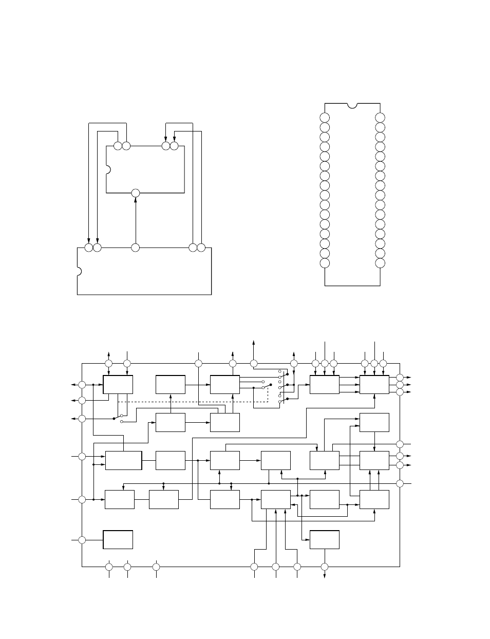
7-3-2. Video/Color Circuit
The video/color circuit consists of two ICs, QV005
(TDA9141: NTSC/PAL/SECAM DECODER), QV006
(TDA4665T: BASE BAND DELAY LINE), and supports
each system of NTSC, PAL and SECAM.
Fig. 7-3-4 shows the pin configuration of TDA9141 and
Fig. 7-3-5 shows the block diagram of TDA9141. Fig. 7-
3-6 shows the pin configuration of TDA4665T and Fig.
7-3-7 shows the block diagram of TDA4665T.
Fig. 7-3-3
Fig. 7-3-4 Pin configuration of TDA9141
Fig. 7-3-5 Block diagram of TDA9141
TDA4665T
(1H DL IC)
Color difference signal
Color difference signal
TDA9141
(NTSC/PAL/SECAM)
Sand castle pulse
12 11
16 14
5
4
3
2
1
10
1
2
4
32
31
30
29
3
5
28
6
27
7
26
8
25
9
24
10
23
11
22
12
21
13
20
14
19
SECAM reference
Second crystal
Reference crystal
CPLL
Filter reference
Analog ground
Y/CVBS in
Cin
HPLL
Fscomb
Address in / CVBS out
R
G
B
-(R-Y)
-(B-Y)
Uin
Vin
SCL
SDA
Supply
Digital supply decoupling
Digital ground
Sand castle
VA
Yout
Vout
Uout
15
18 F
I / O port
16
17 CLP / HA
O port / LLC