Toshiba TLP511E User Manual
Page 35
7-8
7-3-4. Color Signal Process Circuit
The color signal is level adjusted in the ACC (automatic
color control) circuit, corrected in passing through a
band pass circuit in the NTSC/PAL system, or a bell filter
correction is carried out in the SECAM system, and then
enters the color demodulation circuit.
The input burst signal is locked with a crystal oscillator
frequency (3.58 MHz/4.43 MHz) in the PLL circuit and
then demodulated into color difference signals after a
tint adjustment (in the NTSC system). The demodulation
for the SECAM signal is carried out using a PLL circuit.
The demodulated color difference signals are output
through low pass filters, delayed by 1H in passing
through TDA4665T, fed to TDA9141 again and directly
output.
7-3-5. Picture Sharpness Correction Circuit
The picture sharpness is carried out by QV007,
TDA4672. Fig. 7-3-8 shows the pin configuration of
TDA4672 and Fig. 7-3-9 shows the block diagram.
Picture sharpness correction frequency is set to 2.6 MHz.
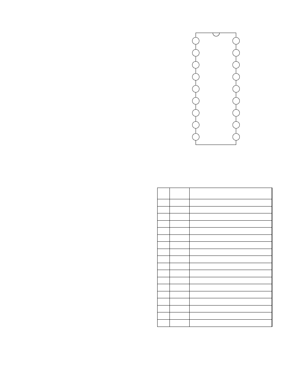
Fig. 7-3-8 Pin configuration of TDA4672
Table 7-3-3 Terminal function of TDA4672
Pin
No.
1
2
3
4
5
6
7
8
9
10
11
12
13
14
15
16
17
18
Name
V
P
C
DL
V
i(R–Y)
V
o(R–Y)
N.C.
V
o(B–Y)
V
i(B–Y)
GND2
SDA
SCL
C
COR
V
o(Y)
C
CLP1
C
CLP2
C
REF
V
i(Y)
SAND
GND1
Function
Positive power supply
Capacitor for delay time control
± (R–Y) color difference input signal
± (R–Y) color difference output signal
Not used
± (B–Y) color difference output signal
± (B–Y) color difference input signal
GND 2 (0V)
I
2
C bus data line
I
2
C bus clock line
Magnetic core capacitor
Delay luminance output signal
Black level clamp capacitor 1
Black level clamp capacitor 2
Reference voltage capacitor
Luminance input signal
Sandcastle pulse input
GND 1 (0V)
GND1
SAND
REF
SCL
C
CLP2
C
CLP1
C
COR
C
N.C.
SDA
P
V
DL
C
MED757
TDA4672
i(Y)
V
o(Y)
V
o(R-Y)
V
i(R-Y)
V
i(B-Y)
V
GND2
o(R-Y)
V
1
2
4
3
5
6
7
8
9
18
17
15
16
14
13
12
11
10