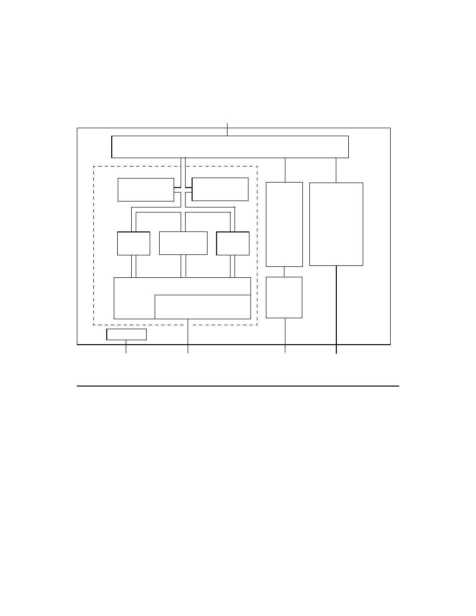
Figure2.1 lsi53c875a block diagram, 1 pci functional description, 1 pci addressing – LSI 53C875A User Manual
Page 24: Pci functional description, Pci addressing, Lsi53c875a block diagram, Section 2.1, “pci functional description, Figure 2.1

2-2
Functional Description
Figure 2.1
LSI53C875A Block Diagram
2.1 PCI Functional Description
The LSI53C875A implements a PCI-to-Wide Ultra SCSI controller.
2.1.1 PCI Addressing
There are three physical PCI-defined address spaces:
•
PCI Configuration space.
•
I/O space for operating registers.
•
Memory space for operating registers.
32 Bit PCI Interface, PCI Configuration Register
4 Kbyte
SCRIPTS RAM
8 Dword SCRIPTS
Prefetch Buffer
944 byte
DMA FIFO
SCSI SCRIPTS
Processor
Operating
Registers
ROM/Flash
Serial EEPROM
Local
Memory
Bus
SCSI FIFO and SCSI Control Block
SE TolerANT
Drivers and Receivers
JTAG
PCI Bus
JTAG Bus
Wide Ultra
SCSI Bus
ROM/Flash
Memory Bus
2-Wire Serial
EEPROM Bus
Wide Ultra SCSI Controller
Controller and
Autoconfiguration
Memory
Control
