Scratch register a (scratcha), Scratch register a, Scratcha) – LSI 53C875A User Manual
Page 157: Dma scripts pointer save, Dsps)

SCSI Registers
4-65
Registers: 0x30–0x33
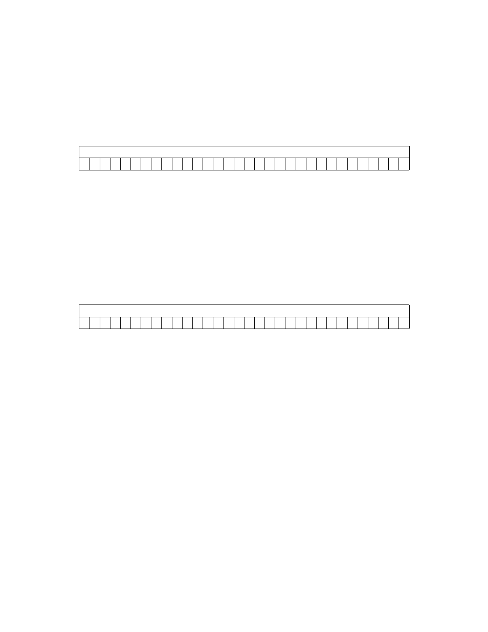
DMA SCRIPTS Pointer Save (DSPS)
Read/Write
DSPS
DMA SCRIPTS Pointer Save
[31:0]
This register contains the second Dword of a SCRIPTS
instruction. It is overwritten each time a SCRIPTS
instruction is fetched. When a SCRIPTS interrupt
instruction is executed, this register holds the interrupt
vector. The power-up value of this register is
indeterminate.
Registers: 0x34–0x37
Scratch Register A (SCRATCHA)
Read/Write
SCRATCHA
Scratch Register A
[31:0]
This is a general purpose, user-definable scratch pad
register. Apart from CPU access, only Register
Read/Write and Memory Moves into the SCRATCH
register alter its contents. The power-up value of this
register is indeterminate.
A special mode of this register is enabled by setting the
PCI Configuration Into Enable bit in the
register. If this bit is set, the SCRATCH A
register returns bits [31:10] of the Memory Mapped
Operating register PCI base address (
) in bits [31:10] of the
when read. Bits [9:0] of SCRATCH
A will always return zero in this mode. Writes to the
SCRATCH A register are unaffected. Clearing the PCI
Configuration Into Enable bit causes the SCRATCH A
register to return to normal operation.
31
0
DSPS
x
x
x
x
x
x
x
x
x
x
x
x
x
x
x
x
x
x
x
x
x
x
x
x
x
x
x
x
x
x
x
x
31
0
SCRATCHA
x
x
x
x
x
x
x
x
x
x
x
x
x
x
x
x
x
x
x
x
x
x
x
x
x
x
x
x
x
x
x
x
