Chip control 0 (ccntl0), Register: 0x56 – LSI 53C875A User Manual
Page 187

SCSI Registers
4-95
Register: 0x56
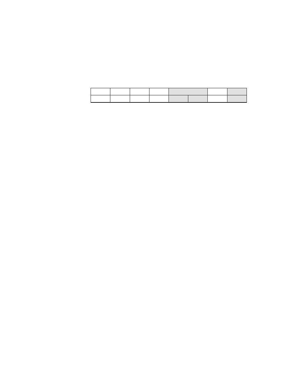
Chip Control 0 (CCNTL0)
Read/Write
ENPMJ
Enable Phase Mismatch Jump
7
Upon setting this bit, any phase mismatches do not
interrupt but force a jump to an alternate location to
handle the phase mismatch. Prior to actually taking the
jump, the appropriate remaining byte counts and
addresses will be calculated such that they can be easily
stored to the appropriate memory location with SCRIPTS
Store instruction.
In the case of a SCSI send, any data in the part will be
automatically cleared after being accounted for. In the
case of a SCSI receive, all data will be flushed out of the
part and accounted for prior to taking the jump. This
feature does not cover, however, the byte that may
appear in
. This byte must
be flushed manually.
This bit also enables the flushing mechanism to flush
data during a Data-In phase mismatch in a more efficient
manner.
PMJCTL
Jump Control
6
This bit controls which decision mechanism is used when
jumping on phase mismatch. When this bit is cleared the
LSI53C875A will use
when the WSR bit is cleared and
Phase Mismatch Jump Address 2 (PMJAD2)
when the
WSR bit is set. When this bit is set the LSI53C875A will
use jump address one (PMJAD1) on data out (data out,
command, message out) transfers and jump address two
(PMJAD2) on data in (data in, status, message in)
transfers. Note that the phase referred to here is the
phase encoded in the block move SCRIPTS instruction,
not the phase on the SCSI bus that caused the phase
mismatch.
7
6
5
4
3
2
1
0
ENPMJ
PMJCTL
ENNDJ
DISFC
R
DILS
R
0
0
0
0
x
x
0
x
