Chip test zero (ctest0), Register: 0x18, Register: 0x19 – LSI 53C875A User Manual
Page 145

SCSI Registers
4-53
Register: 0x18
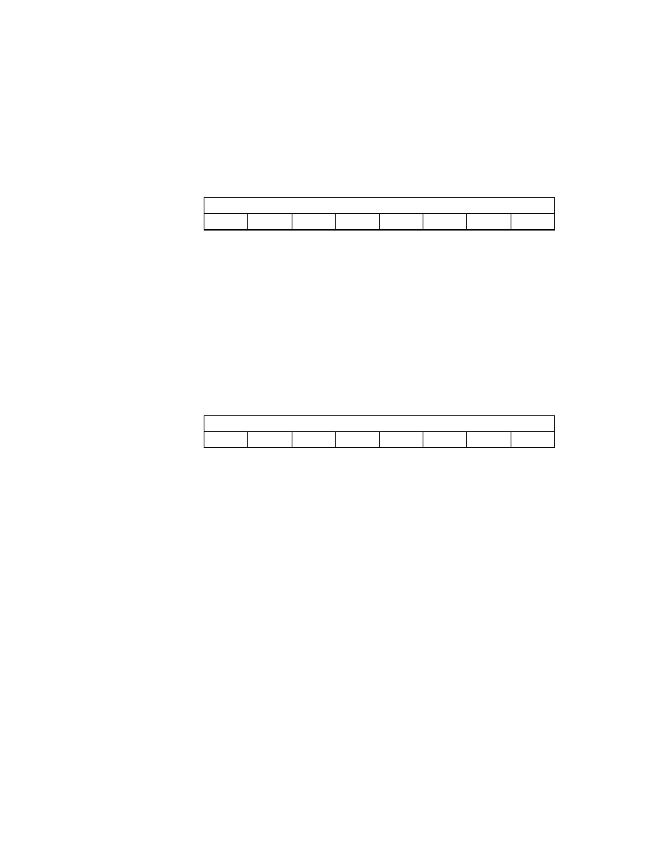
Chip Test Zero (CTEST0)
Read/Write
FMT
Byte Empty in DMA FIFO
[7:0]
These bits identify the bottom bytes in the DMA FIFO that
are empty. Each bit corresponds to a byte lane in the
DMA FIFO. For example, if byte lane three is empty, then
FMT3 will be set. Since the FMT flags indicate the status
of bytes at the bottom of the FIFO, if all FMT bits are set,
the DMA FIFO is empty.
Register: 0x19
Chip Test One (CTEST1)
Read Only
FFL
Byte Full in DMA FIFO
[7:0]
These status bits identify the top bytes in the DMA FIFO
that are full. Each bit corresponds to a byte lane in the
DMA FIFO. For example, if byte lane three is full then
FFL3 is set. Since the FFL flags indicate the status of
bytes at the top of the FIFO, if all FFL bits are set, the
DMA FIFO is full.
7
0
FMT
1
1
1
1
1
1
1
1
7
0
FFL
0
0
0
0
0
0
0
0
