Pll frequency synthesizer, Control circuit, Tk-7150 – Kenwood TK-7150 User Manual
Page 14: Circuit description
TK-7150
14
3-4. Automatic Power Control, Circuit and Transmitter
The automatic power control (APC) circuit stabilizes the
transmitter output power at a predetermined level, and con-
sists of forward/reflected power detector circuits. The for-
ward/reflected power detector circuits detects forward RF
power and reflected RF power to DC voltage, and consists of
a C coupling type detection circuit, RF detector D5/D6, and
DC amplifier IC2 (A/2).
The voltage comparator (IC2 B/2) compares the voltage
obtained by the above detected voltage with a reference volt-
age, set using the microprocessor and IC718 and IC715.
An APC voltage proportional to the difference between
the sensed voltage and the reference voltage appears at the
output of IC2. This output voltage controls the gate voltage
for the drive amplifier Q4 and final amplifier Q5, which keeps
the transmitter output power constant.
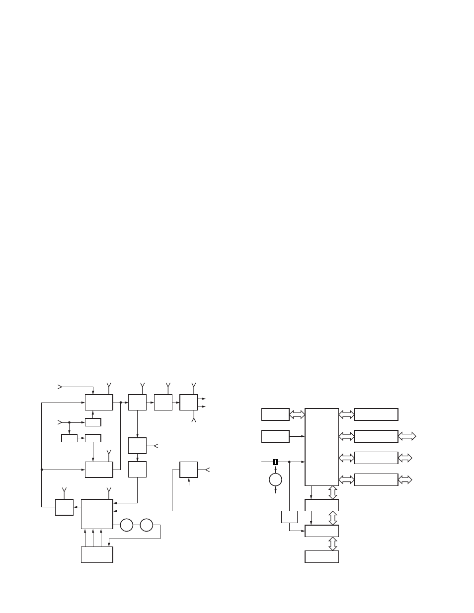
4. PLL Frequency Synthesizer
The transmit signal and the receive first L.O. signal are
generated by the PLL digital frequency synthesizer. The fre-
quency synthesizer consists of a transmitter voltage con-
trolled oscillator (TX VCO; Q507), a receiver voltage con-
trolled oscillator (RX VCO; Q509), a buffer amplifier (Q513
and Q515), an RF amplifier (Q516), a low-pass filter (Q501,
Q503 and Q504), a PLL IC (IC501), and TX VCO/RX VCO
switches (Q510 and Q512).
In the transmit signal mode, an operating frequency pro-
gramming data is sent to IC501, from the CPU (IC701), to set
the programmable counter within IC501. Q512 is turned on
to activate the TX VCO and the output signal of the TX VCO is
amplified by Q513 and Q516.
The signal is then divided down in frequency, at the pro-
grammable counter in IC501, to 5.0kHz or 6.25kHz, 7.5kHz
which is compared in phase with a 5.0kHz or 6.25kHz, 7.5kHz
reference signal, derived from 16.8MHz VCXO (X501) and a
Q507
BUFF
AMP
BUFF
AMP
AMP
SW
TX VCO
SW Q512
SW
SW
Q510
Q514
8CL
8CL
8C
8T
8R
Q509
RX VCO
8CL
PLL IC
IC701
CPU
8CL
STR
MO
5C
Q516
VCXO
5C
X501
16.8MHz
Q513
Q515
LPF
LPF
12CL
Q501
Q503
Q504
D513
D514
TX
RX
IC501
SW
SW
Q518
Q519
DT
CP
EP
UL
MB
Fig. 4
PLL circuit
1/3360 or a 1/2688, 1/2240 fixed counter in IC501, at the
phase comparator in IC501. The VCXO operates at 16.8MHz
and its frequency stability is maintained within 2.5ppm (tem-
perature range of –30 to +60 degrees).
The phase comparator output signal is fed into a low-pass
filter (Q501, Q503 and Q504) before being applied tot the TX
vco as a frequency control voltage. This low-pass filter’s
power is supplied by the DC/DC converter (Q502, Q505,
Q506, Q508, and Q511). If an unlock condition occurs in the
phase locked loop, this condition is detected by Q518 and
Q519. This cause the transmitter 8V supply cut off, resulting
in the prevention of an unauthorized transmission.
The transmitter modulation signals (processed Mic. audio
and sub-audible signalling) are applied to the TX VCO for fre-
quency modulation.
In the receive mode, the VCO is substituted with Q509
(RX VCO) and it generates the receiver first local oscillator
signal according to the data sent from the CPU (IC701). The
basic operation of the synthesizer remains the same.
5. Control Circuit
The control circuit mainly consists of CPU, memory cir-
cuit, DSP circuit, and power supply circuit.
5-1. CPU
The CPU (IC701) controls the flash ROM (IC705), the DSP
(IC710), the receiver circuit, the transmitter circuit, the con-
trol circuit, and the display circuit and transfers data to or
from an external device.
5-2. Memory Circuit
IC705 has a flash ROM with a capacity of 4M bits that
contains the control program for the CPU, the signal process-
ing program for DSP and data such as channels and operating
features.
This program can be easily written from an external de-
vices. Data such as the operating status are programmed
into the EEPROM (IC704).
IC700/702
EEPROM
Reset IC
Shift register IC
IC718
D/A IC
IC703
232C driver
IC705
IC704
IC103
Flash ROM
Interface IC
IC701
CPU
IC706~709
DSP
IC710
CODEC IC
IC713
INV
IC711
SW
X700
12.288MHz
Q700
BEAT
SHIFT
Fig. 5
Control circuit
CIRCUIT DESCRIPTION