Transmitter circuit, Tk-7150, Circuit description – Kenwood TK-7150 User Manual
Page 13
TK-7150
13
2-4. Audio Amplifier
The recovered audio signal obtained from IC201 is ampli-
fied and anti-aliasing filtered by IC712 (A/2), inputted to the
AINR terminal of CODEC IC (IC713), and audio processed by
DSP (IC710). The processed audio signal from AOUTR termi-
nal of IC713 is amplified and filtered by IC716 (A/2) to a suffi-
cient level. The audio signal goes to an electronic volume
(IC718) and then it passes through the amplifier (IC722), to
the input of multiplexer IC (IC717), and is amplified to drive a
loudspeaker by an audio power amplifier (IC720). The audio
output can be provided to external 4Ω speaker through the 6-
pin ACC connector “ES1, ES2” on the rear panel. Q711 is a
mute switch.
2-5. Squelch Circuit
The output signal from IC201 enters FM IC again, then
passed through a band-pass filter.
The noise component output from IC201 is amplified by
Q204 and rectified by D202 to produce a DC Voltage corre-
sponding to the noise level. The DC voltage is sent to the
analog port of the CPU (IC701).
IC201 outputs a DC voltage (RSSI) corresponding to the
input of the IF amplifier.
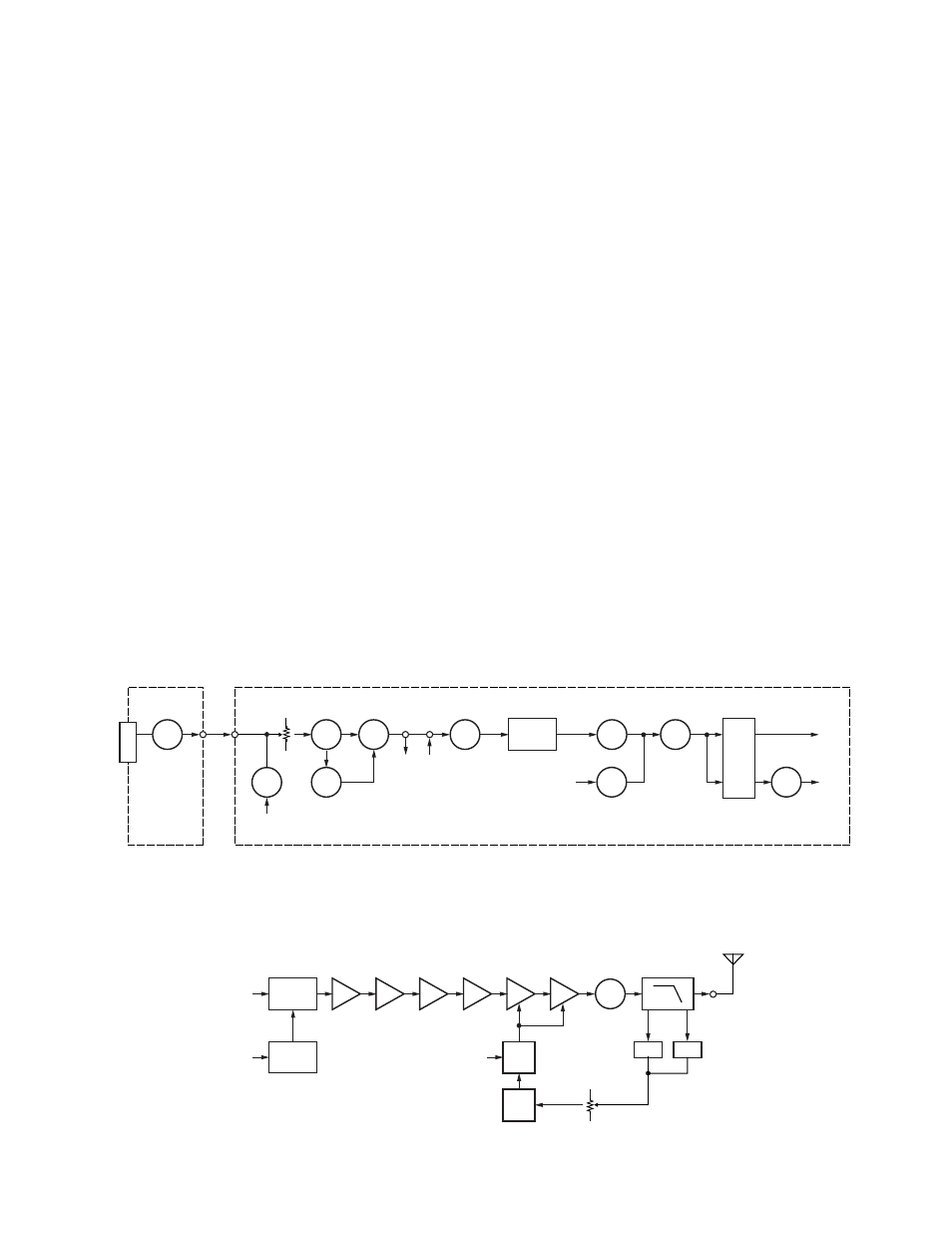
3. Transmitter Circuit
The transmitter circuit consists of the following circuits : 3-
1 microphone circuit, 3-2 modulation level adjustment circuit,
3-3 driver and final power amplifier circuit, and 3-4 automatic
power control circuit.
3-1. Microphone Circuit
The signal from the microphone passes through the mute
switch (Q901) and is then routed to the Display unit (X54-340)
and TX-RX unit (X57-657). The signal then passes through
the AGC circuit to avoid signal distortion.
This circuit consists of IC714, D711, D712, Q707, and
Q708. The AGC is operated by controlling the + and – side
levels of amplitude using the current obtained by positive and
negative detection of the amplified audio signal.
The audio signal is amplified by IC712 (B/2), input to the
AINL terminal of CODEC IC (IC713), and audio processed by
DSP (IC710). The processed audio signal from the AOUTL
terminal of IC713 is amplified and filtered by IC716 (B/2), and
amplified by the summing amplifier IC719 (B/2).
3-2. Modulation Level Adjustment Circuit
The output of the summing amplifier IC719 (B/2) is passed
to an electronic volume (IC718) for maximum deviation ad-
justment before being applied to a varactor diode in the volt-
age controlled oscillator VCO.
3-3. Driver and Final Power Amplifier Circuit
The transmit signal is generated by the TX VCO (Q507),
amplified by Q513 and Q 515. This amplified signal is ampli-
fied by Q1, Q2, Q4, and Q5. And this signal is passed to the
FINAL stage. The RF power amplifier consists of MOS FET
transistor.
AMP
DET
SW
IC714
(A/2)
ATT
Q707,708
SW
Q901
AMP
IC712
(B/2)
LPF
IC716
(B/2)
AMP
IC719
(B/2)
DC
AMP
IC715
(B/2)
SW
IC717
IC718
IC713
D711,712
IC717
VR700
D-SUB
MI2
TXO TXI
AINL
CODEC
IC
AOUTL
D-SUB
DI
DAC
MB
MO
MIC
J901
MIC jack
DISPLAY UNIT
(X54-340)
TX-RX UNIT (X57-657)
TX VCO
VCXO
16.8MHz
Q507
Q1
Drive
AMP
Q513
Buff
AMP
Q515
Buff
AMP
Q2
Drive
AMP
Q4
Drive
AMP
Q5
Final
AMP
X501
MO
MB
REF
AMP
DC
AMP
Vcont
IC2
(B/2)
IC2
(A/2)
PC
SW
D3
DET
DET
VR1
Power adj.
D5
D6
ANT
Fig. 2
Microphone circuit
Fig. 3
Drive and final amplifier circuit
CIRCUIT DESCRIPTION