Instruction set summary – Intel 80L186EA User Manual
Page 49
80C186EA 80C188EA 80L186EA 80L188EA
INSTRUCTION SET SUMMARY
(Continued)
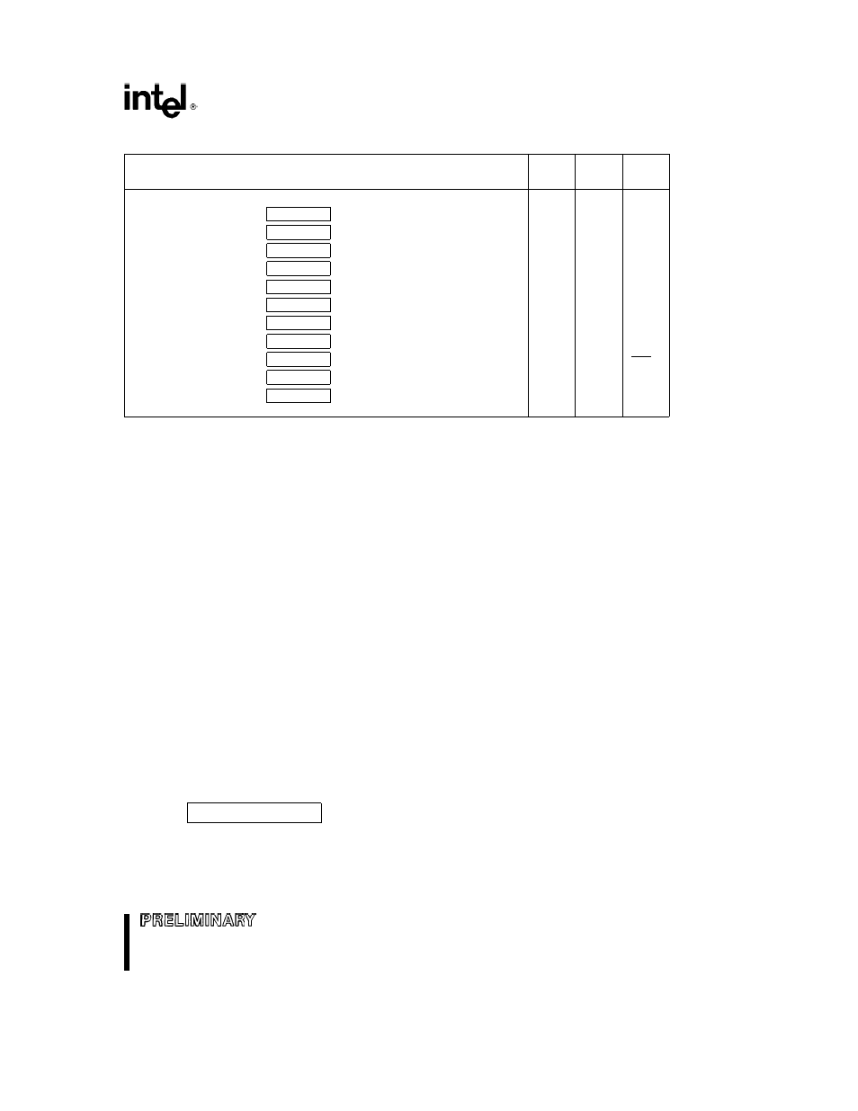
Function
Format
80C186EA
80C188EA
Comments
Clock
Clock
Cycles
Cycles
PROCESSOR CONTROL
CLC
e
Clear carry
1 1 1 1 1 0 0 0
2
2
CMC
e
Complement carry
1 1 1 1 0 1 0 1
2
2
STC
e
Set carry
1 1 1 1 1 0 0 1
2
2
CLD
e
Clear direction
1 1 1 1 1 1 0 0
2
2
STD
e
Set direction
1 1 1 1 1 1 0 1
2
2
CLI
e
Clear interrupt
1 1 1 1 1 0 1 0
2
2
STI
e
Set interrupt
1 1 1 1 1 0 1 1
2
2
HLT
e
Halt
1 1 1 1 0 1 0 0
2
2
WAIT
e
Wait
1 0 0 1 1 0 1 1
6
6
if TEST
e
0
LOCK
e
Bus lock prefix
1 1 1 1 0 0 0 0
2
2
NOP
e
No Operation
1 0 0 1 0 0 0 0
3
3
(TTT LLL are opcode to processor extension)
Shaded areas indicate instructions not available in 8086 8088 microsystems
NOTE
Clock cycles shown for byte transfers For word operations add 4 clock cycles for all memory transfers
The Effective Address (EA) of the memory operand
is computed according to the mod and r m fields
if mod
e
11 then r m is treated as a REG field
if mod
e
00 then DISP
e
0
disp-low and disp-
high are absent
if mod
e
01 then DISP
e
disp-low sign-ex-
tended to 16-bits disp-high is absent
if mod
e
10 then DISP
e
disp-high disp-low
if r m
e
000 then EA
e
(BX)
a
(SI)
a
DISP
if r m
e
001 then EA
e
(BX)
a
(DI)
a
DISP
if r m
e
010 then EA
e
(BP)
a
(SI)
a
DISP
if r m
e
011 then EA
e
(BP)
a
(DI)
a
DISP
if r m
e
100 then EA
e
(SI)
a
DISP
if r m
e
101 then EA
e
(DI)
a
DISP
if r m
e
110 then EA
e
(BP)
a
DISP
if r m
e
111 then EA
e
(BX)
a
DISP
DISP follows 2nd byte of instruction (before data if
required)
except if mod
e
00 and r m
e
110 then EA
e
disp-high disp-low
EA calculation time is 4 clock cycles for all modes
and is included in the execution times given whenev-
er appropriate
Segment Override Prefix
0
0
1
reg
1
1
0
reg is assigned according to the following
Segment
reg
Register
00
ES
01
CS
10
SS
11
DS
REG is assigned according to the following table
16-Bit (w
e
1)
8-Bit (w
e
0)
000 AX
000 AL
001 CX
001 CL
010 DX
010 DL
011 BX
011 BL
100 SP
100 AH
101 BP
101 CH
110 SI
110 DH
111 DI
111 BH
The physical addresses of all operands addressed
by the BP register are computed using the SS seg-
ment register The physical addresses of the desti-
nation operands of the string primitive operations
(those addressed by the DI register) are computed
using the ES segment which may not be overridden
49
49