Intel 80L186EA User Manual
Page 23
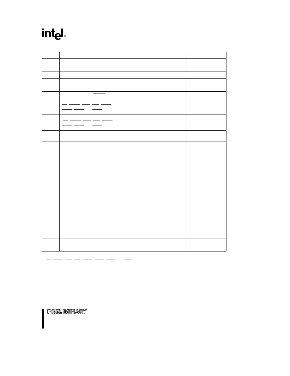
80C186EA 80C188EA 80L186EA 80L188EA
DC SPECIFICATIONS (80L186EA 80L188EA)
Symbol
Parameter
Min
Max
Units
Conditions
V
CC
Supply Voltage
2 7
5 5
V
V
IL
Input Low Voltage for All Pins
b
0 5
0 3 V
CC
V
V
IH
Input High Voltage for All Pins
0 7 V
CC
V
CC
a
0 5
V
V
OL
Output Low Voltage
0 45
V
I
OL
e
1 6 mA (min)
V
OH
Output High Voltage
V
CC
b
0 5
V
I
OH
e b
1 mA (min)
V
HYR
Input Hysterisis on RESIN
0 30
V
I
IL1
Input Leakage Current (except
g
10
m
A
0V
s
V
IN
s
V
CC
RD QSMD UCS LCS MCS0 PEREQ
MCS1 LOCK and TEST)
I
IL2
Input Leakage Current
b
275
m
A
V
IN
e
0 7 V
CC
(RD QSMD UCS LCS MCS0
(Note 1)
MCS1 LOCK and TEST)
I
OL
Output Leakage Current
g
10
m
A
0 45
s
V
OUT
s
V
CC
(Note 2)
I
CC5
Supply Current (RESET 5 5V)
80L186EA-13
65
mA
(Note 3)
80L186EA-8
40
mA
(Note 3)
I
CC3
Supply Current (RESET 2 7V)
80L186EA-13
34
mA
(Note 3)
80L186EA-8
20
mA
(Note 3)
I
ID5
Supply Current Idle (5 5V)
80L186EA-13
46
mA
80L186EA-8
28
mA
I
ID5
Supply Current Idle (2 7V)
80L186EA-13
24
mA
80L186EA-8
14
mA
I
PD5
Supply Current Powerdown (5 5V)
80L186EA-13
100
m
A
80L186EA-8
100
m
A
I
PD3
Supply Current Powerdown (2 7V)
80L186EA-13
50
m
A
80L186EA-8
50
m
A
C
OUT
Output Pin Capacitance
0
15
pF
T
F
e
1 MHz (Note 4)
C
IN
Input Pin Capacitance
0
15
pF
T
F
e
1 MHz
NOTES
1 RD QSMD UCS LCS MCS0 MCS1 LOCK and TEST have internal pullups that are only activated during RESET
Loading these pins above I
OL
e b
275 mA will cause the processor to enter alternate modes of operation
2 Output pins are floated using HOLD or ONCE Mode
3 Measured at worst case temperature and V
CC
with all outputs loaded as specified in the AC Test Conditions and with the
device in RESET (RESIN held low)
4 Output capacitance is the capacitive load of a floating output pin
23
23