Intel 80L186EA User Manual
Page 10
80C186EA 80C188EA 80L186EA 80L188EA
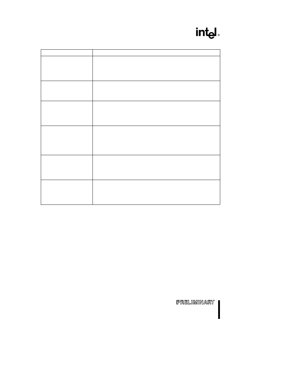
Table 2 Pin Description Nomenclature
Symbol
Description
P
Power Pin (Apply
a
V
CC
Voltage)
G
Ground (Connect to V
SS
)
I
Input Only Pin
O
Output Only Pin
I O
Input Output Pin
S(E)
Synchronous Edge Sensitive
S(L)
Synchronous Level Sensitive
A(E)
Asynchronous Edge Sensitive
A(L)
Asynchronous Level Sensitive
H(1)
Output Driven to V
CC
during Bus Hold
H(0)
Output Driven to V
SS
during Bus Hold
H(Z)
Output Floats during Bus Hold
H(Q)
Output Remains Active during Bus Hold
H(X)
Output Retains Current State during Bus Hold
R(WH)
Output Weakly Held at V
CC
during Reset
R(1)
Output Driven to V
CC
during Reset
R(0)
Output Driven to V
SS
during Reset
R(Z)
Output Floats during Reset
R(Q)
Output Remains Active during Reset
R(X)
Output Retains Current State during Reset
I(1)
Output Driven to V
CC
during Idle Mode
I(0)
Output Driven to V
SS
during Idle Mode
I(Z)
Output Floats during Idle Mode
I(Q)
Output Remains Active during Idle Mode
I(X)
Output Retains Current State during Idle Mode
P(1)
Output Driven to V
CC
during Powerdown Mode
P(0)
Output Driven to V
SS
during Powerdown Mode
P(Z)
Output Floats during Powerdown Mode
P(Q)
Output Remains Active during Powerdown Mode
P(X)
Output Retains Current State during Powerdown Mode
10
10