Intel 80L186EA User Manual
Page 17
80C186EA 80C188EA 80L186EA 80L188EA
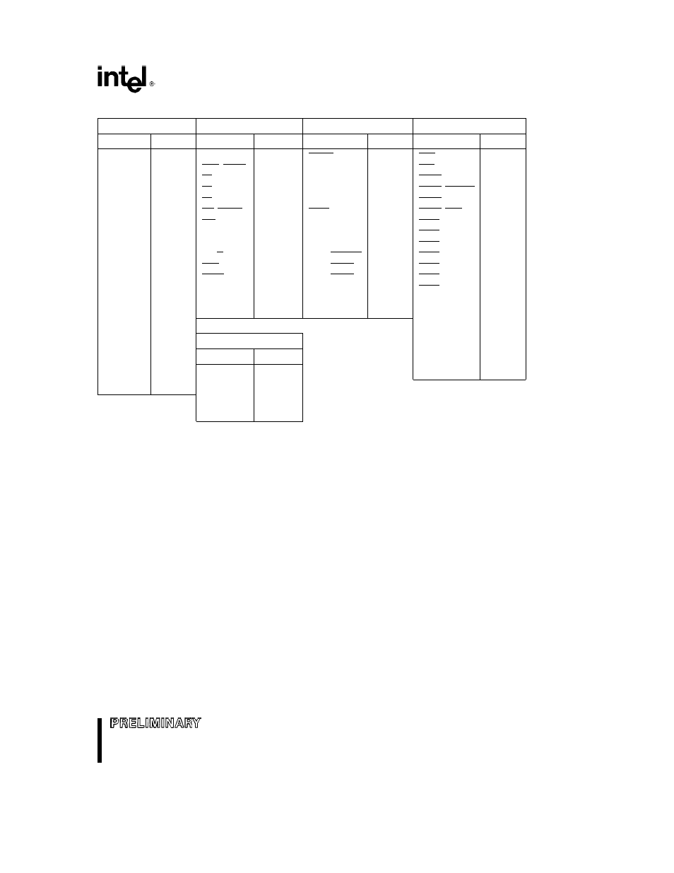
Table 6 QFP (EIAJ) Pin Names with Package Location
Address Data Bus
Bus Control
Processor Control
I O
Name
Location
Name
Location
Name
Location
Name
Location
AD0
64
ALE QS0
10
RESIN
55
UCS
45
AD1
66
BHE (RFSH)
7
RESOUT
18
LCS
46
AD2
68
S0
23
CLKIN
16
MCS0 PEREQ
40
AD3
70
S1
22
OSCOUT
17
MCS1 ERROR
41
AD4
74
S2
21
CLKOUT
19
MCS2
42
AD5
76
RD QSMD
9
TEST BUSY
29
MCS3 NCS
43
AD6
78
WR QS1
8
PDTMR
38
PCS0
54
AD7
80
ARDY
20
NMI
30
PCS1
52
AD8 (A8)
65
SRDY
27
INT0
31
PCS2
51
AD9 (A9)
67
DT R
37
INT1 SELECT
32
PCS3
50
AD10 (A10)
69
DEN
39
INT2 INTA0
35
PCS4
49
AD11 (A11)
71
LOCK
28
INT3 INTA1
36
PCS5 A1
48
AD12 (A12)
75
HOLD
26
IRQ
PCS6 A2
47
AD13 (A13)
77
HLDA
25
N C
11 14
T0OUT
57
AD14 (A14)
79
15 63
T0IN
59
AD15 (A15)
1
T1OUT
56
A16
3
Power
T1IN
58
A17
4
Name
Location
DRQ0
61
A18
5
V
SS
12 13 24
DRQ1
60
A19 S6
6
53 62
V
CC
2 33 34
44 72 73
NOTE
Pin names in parentheses apply to the 80C186EA 80L188EA
17
17