Intel 80L186EA User Manual
Page 12
80C186EA 80C188EA 80L186EA 80L188EA
Table 3 Pin Descriptions
(Continued)
Pin
Pin
Input
Output
Description
Name
Type
Type
States
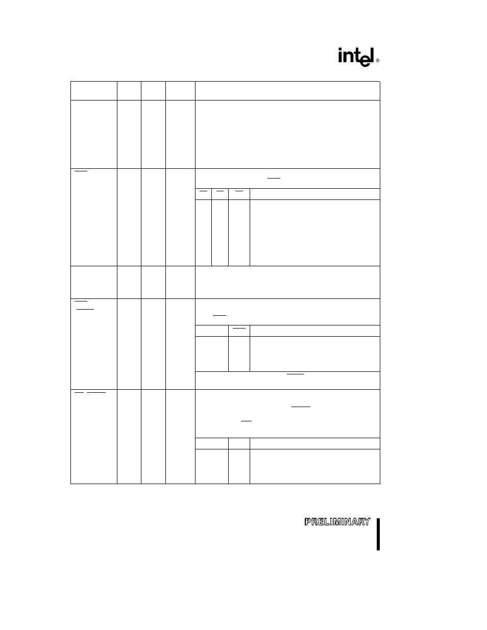
A18 16
O
H(Z)
These pins provide multiplexed Address during the address
phase of the bus cycle Address bits 16 through 19 are
A19 S6 – A16
R(Z)
presented on these pins and can be latched using ALE
(A19 – A8)
P(X)
A18 16 are driven to a logic 0 during the data phase of the bus
cycle On the 8-bit bus versions A15 – A8 provide valid address
information for the entire bus cycle Also during the data
phase S6 is driven to a logic 0 to indicate a CPU-initiated bus
cycle or logic 1 to indicate a DMA-initiated bus cycle or a
refresh cycle
S2 0
O
H(Z)
Bus cycle Status are encoded on these pins to provide bus
transaction information S2 0 are encoded as follows
R(Z)
P(1)
S2
S1
S0
Bus Cycle Initiated
0
0
0
Interrupt Acknowledge
0
0
1
Read I O
0
1
0
Write I O
0
1
1
Processor HALT
1
0
0
Queue Instruction Fetch
1
0
1
Read Memory
1
1
0
Write Memory
1
1
1
Passive (no bus activity)
ALE QS0
O
H(0)
Address Latch Enable
output is used to strobe address
information into a transparent type latch during the address
R(0)
phase of the bus cycle In Queue Status Mode QS0 provides
P(0)
queue status information along with QS1
BHE
O
H(Z)
Byte High Enable
output to indicate that the bus cycle in
progress is transferring data over the upper half of the data
(RFSH)
R(Z)
bus BHE and A0 have the following logical encoding
P(X)
A0
BHE
Encoding (For 80C186EA 80L186EA Only)
0
0
Word Transfer
0
1
Even Byte Transfer
1
0
Odd Byte Transfer
1
1
Refresh Operation
On the 80C188EA 80L188EA RFSH is asserted low to
indicate a Refresh bus cycle
RD QSMD
O
H(Z)
ReaD
output signals that the accessed memory or I O device
must drive data information onto the data bus Upon reset this
R(WH)
pin has an alternate function As QSMD it enables Queue
P(1)
Status Mode
when grounded In Queue Status Mode the
ALE QS0 and WR QS1 pins provide the following information
about processor instruction queue interaction
QS1
QS0
Queue Operation
0
0
No Queue Operation
0
1
First Opcode Byte Fetched from the Queue
1
1
Subsequent Byte Fetched from the Queue
1
0
Empty the Queue
NOTE
Pin names in parentheses apply to the 80C188EA and 80L188EA
12
12