4 rf input switch j6 connector, 3 rf interface connectors, 1 rf in 1 j7, rf in 2 j8 connectors – Comtech EF Data PCB-4300 User Manual
Page 28: 2 sspa out 1 j9 connector
PCB-4300 1:2 Phase Combiner
Revision 2
External Connectors
MN/PCB4300.IOMMN/PCB4300.IOM
2–6
2.2.4
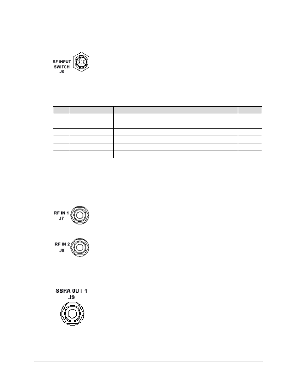
RF INPUT SWITCH J6 Connector
The PCCB contains a built-in selector switch, a latching 28 VDC coaxial
unit. The position of this switch is selected by the RF INPUT SWITCH J6
– a 6-pin circular connector (CEFD P/N CN/MS-PT07M6PC). Its pinout
specification is provided in Table 2-5.
Mating connector: ITT Cannon MS3116J10-6S
(CEFD P/N CN/MS3116J10-6S).
Table 2-5. Connector J6 Pinouts
Pin # Signal Function
Signal Name / Description
Direction
A
POS1, Drive
Input
B
Ground GND
C
POS2, Drive
Input
D
POS1, Indicator
Output
E
Ground GND
F
POS2, Indicator
Output
2.3
RF Interface Connectors
2.3.1
RF IN 1 J7, RF IN 2 J8 Connectors
The RF IN 1 J7 and RF IN 2 J8 connectors are Type ‘N’ female connectors,
each serving as an RF signal input interface to the PCCB. Note the following:
• The RF IN 1 J7 input is selected when the RF INPUT SWITCH J6’s
“POS1” Signal Function is activated.
• The RF IN 2 J8 input is selected when the RF INPUT SWITCH J6’s
“POS2” Signal Function is activated.
2.3.2
SSPA OUT 1 J9 Connector
The SSPA OUT J10 connector, located on the left side panel of the PCCB, is
a Type ‘N’ female connector. It provides the RF signal output from the PCCB
to SSPA #1.