3 ps, synthesizer, and d/c, p4 db25-male – Comtech EF Data CST-5005 User Manual
Page 77
CST-5005 C-Band Satellite Terminal
Theory of Operation
Rev. 1
5–7
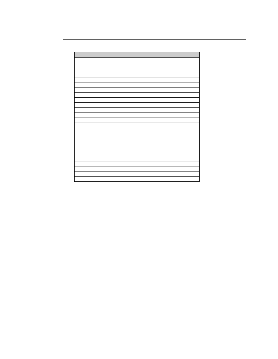
5.1.5.3 PS, Synthesizer, and D/C, P4 DB25-Male
Pin #
Name
Description
1
HPA 12V
Input, 12.5V power from PS
14
HPA 12V
Input, 12.5V power from PS
2
UC 12V
Input, 12.5V power from PS
15
M&C 12V
Input, 12.5V power from PS
3
SYN DATA
Output CMOS level, Data
16
SYN CLOCK
Output CMOS level, Clock
4
SYN EN1
Output CMOS level, Enable 1
17
SYN EN2
Output CMOS level, Enable 2
5
SYN EN3
Output CMOS level, Enable 3
18
IFLO LD
Input, Open collector, floating = fault
6
SYN LD
Input, Open collector, floating = fault
19
2ND SYN LD
Input, Open collector, floating = fault
7
OSC FLT
Input, Open collector, floating = fault
20
RNG_SW
Output, CMOS level, range select
8
DC THERM
Input, 5K thermistor tied to ground
21
SYN EN 4
Output, CMOS, Enable 4
9
DC GAIN CNTL
Output, 0 to 5V
22
SDA
Bidirectional, CMOS serial data
10
SCL
Output, CMOS serial clock
23
LNA PWR
Output, 11V power to the LNA coax
11
FREQ CNTL
Output, 0 to 10V
24
M&C GND
Ground
12
UC GND
Ground
25
HPA GND
Ground
13
HPA GND
Ground
- CDD-880 (124 pages)
- CDM-800 (130 pages)
- ODMR-840 (184 pages)
- CDM-750 (302 pages)
- CDM-840 (244 pages)
- SLM-5650A (420 pages)
- CTOG-250 (236 pages)
- CDM-700 (256 pages)
- CDM-760 (416 pages)
- CDM-710G (246 pages)
- CDM-600/600L (278 pages)
- CDMR-570L (512 pages)
- CDM-625 (684 pages)
- CDM-625A (756 pages)
- CDD-564A (240 pages)
- CDD-564L (254 pages)
- CLO-10 (134 pages)
- MCED-100 (96 pages)
- CDMR-570AL (618 pages)
- CDM-600 LDPC (2 pages)
- BUC Power Supply Ground Cable (2 pages)
- MPP70 Hardware Kit for CDM-570L (4 pages)
- MPP50 Hardware Kit for CDM-570L (4 pages)
- CDM-625 DC-AC Conversion (4 pages)
- CDM-625 DC-AC Conversion with IP Packet Processor (4 pages)
- DMDVR20 LBST Rev 1.1 (117 pages)
- DMD2050E (212 pages)
- DMD-2050 (342 pages)
- DMD1050 (188 pages)
- OM20 (220 pages)
- QAM256 (87 pages)
- DD240XR Rev Е (121 pages)
- MM200 ASI Field (5 pages)
- DM240-DVB (196 pages)
- MM200 (192 pages)
- CRS-150 (78 pages)
- CRS-280L (64 pages)
- CRS-170A (172 pages)
- CRS-180 (136 pages)
- SMS-301 (124 pages)
- CiM-25/8000 (186 pages)
- CiM-25 (26 pages)
- CRS-500 (218 pages)
- CRS-311 (196 pages)
- CIC-20 LVDS to HSSI (26 pages)