Clock structure, 1 overview, Table 5-1 – Artesyn COMX-P40x0 ENP2 Installation and Use (January 2015) User Manual
Page 89: Figure 5-1, Clock distribution, Chapter 5
Chapter 5
COMX-P40x0 ENP2 Installation and Use (6806800R95C)
89
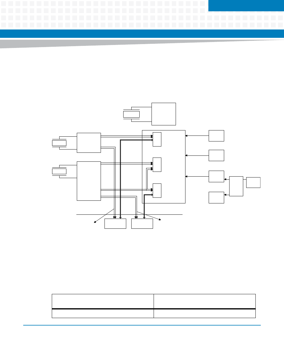
Clock Structure
5.1
Overview
The COMX-P40x0 ENP2 module require several kinds of single ended and differential clocks for
booting up and normal operation. Following is the clock distribution tree:
The output frequency of the bank 1 and bank 2/3 SerDes clocks is selectable between 100 MHz
and 125 MHz. This must be set correctly by the carrier or corresponding CPU GPIO pins
depending on what RCW SerDes configuration is selected. For proper settings, refer
.
Figure 5-1
Clock Distribution
Table 5-1 Configuration of the frequency of SerDes reference clock by carrier
SerDes bank 1 reference clock select (pin B97 on
COM Express)
SerDes bank 2/3 reference clock select (pin B98
on COM Express)
Bank1_SEL_FS0=0, 100 MHz
Bank2_SEL_S1=0, 100 MHz
Bank 1
Bank 2
Bank 3
GE PHY
Crystal
ICS9FG104
(<50ps)
Crystal
ICS9FG104
(<50ps)
Crystal
100 MHz
OSC
RTC
32.768 KHz
24 MHz
OSC
USB
PHY
Device on
Carrier
COME Connector
100 MHz
100 MHz
125 MHz
USB
PHY
CY2305
Device on
Carrier
125 MHz
P40x0
100 MHz
32.768 KHz
60 MHz
24 MHz
Reference clock for
Bank 2#/3#
Reference clock
for Bank 1#
- ARTM-9405 16x10GbE Installation and Use Guide (May 2014) (64 pages)
- ATCA 7370 / ATCA 7370-S Installation and Use (January 2015) (256 pages)
- ATCA 7370 / ATCA 7370-S Installation and Use (September 2014) (254 pages)
- ARTM-831X Installation and Use (June 2014) (346 pages)
- ATCA-7350 - Integrating with Workbench User Guide (September 2014) (34 pages)
- ATCA-7350 Installation and Use (September 2014) (208 pages)
- ATCA-7365-CE Installation and Use (May 2014) (306 pages)
- ATCA-7365-CE Installation and Use (Jan 2015) (300 pages)
- ATCA-7365-CE Installation and Use (May 2014) (294 pages)
- ATCA-7368 Installation and Use (June 2014) (222 pages)
- ATCA-7475 Installation and Use (October 2014) (284 pages)
- ATCA-7480 Installation and Use (April 2015) (330 pages)
- ATCA-8330 Installation and Use (April 2015) (236 pages)
- ATCA-8320 Installation and Use (May 2014) (456 pages)
- ATCA-9305 User's Manual (May 2014) (270 pages)
- ATCA-9405 Installation and Use (October 2014) (168 pages)
- ATCA-F120 Installation and Use (August 2014) (122 pages)
- ATCA-F140 Installation and Use (September 2014) (138 pages)
- ATCA-MF106 Installation and Use (September 2014) (86 pages)
- Centellis-4440/AXP1440 Installation and Use (September 2014) (208 pages)
- Centellis 4410 (AXP-1410) Installation and Use (July 2014) (202 pages)
- Centellis 2100 Release 3.0 Installation and Use (March 2015) (192 pages)
- Centellis 2100 Release 3.0 Installation and Use (March 2015) (176 pages)
- Centellis 2000 User Card-10GE Installation and Use (May 2014) (54 pages)
- Centellis 2000 User Card-10GE with Telco Alarm Installation and Use (May 2014) (60 pages)
- COMX-CAR-210 Installation and Use (August 2014) (76 pages)
- COMX-P1022 Installation and Use (July 2014) (84 pages)
- COMX-P2020 Installation and Use (February 2015) (100 pages)
- COMX-CORE Series Installation and Use (August 2014) (128 pages)
- COMX-P2020 Installation and Use (July 2014) (100 pages)
- COMX-P4080-2G-ENP2 Installation and Use (August 2014) (70 pages)
- COMX-P4080 Installation and Use (August 2014) (126 pages)
- COMX-P40x0 ENP2 Installation and Use (August 2014) (130 pages)
- iVPX7225 RTM Installation and Use (April 2015) (56 pages)
- MITX-430/MITX-440-DVI-2E Installation and Use (August 2014) (118 pages)
- CPCI-6200 Installation and Use (May 2015) (234 pages)
- SCP-MITX-CORE-820-SM Installation and Use (August 2014) (132 pages)
- iVPX7225 Installation and Use (April 2015) (168 pages)
- MVME2502 Installation and Use (December 2014) (166 pages)
- MVME2502 Installation and Use (August 2014) (150 pages)
- MVME2500 VxWorks 6.8 AMP User Guide (August 2014) (40 pages)
- MVME2500 VxWorks 6.8 User Guide (April 2014) (44 pages)
- MVME3100 Single Board Computer Installation and Use (June 2014) (156 pages)
- MVME4100 Single Board Computer Installation and Use (June 2014) (136 pages)