2 memory map, Table 4-4, Memory map – Artesyn COMX-P40x0 ENP2 Installation and Use (January 2015) User Manual
Page 77: Functional description
Functional Description
COMX-P40x0 ENP2 Installation and Use (6806800R95C)
77
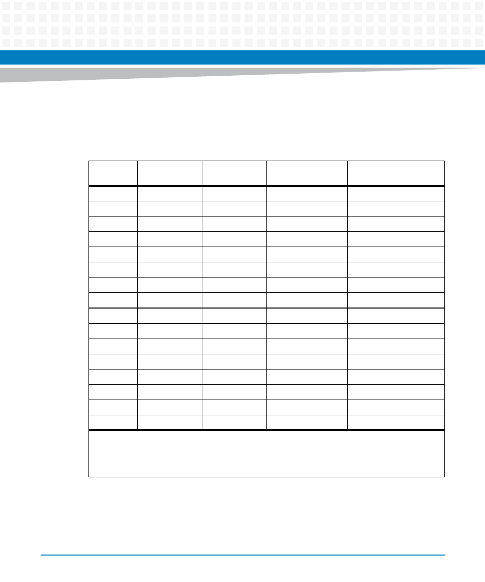
4.8.2
Memory Map
The following table provides the U-boot memory map of the COMX-P40x0 ENP2.
Table 4-4 Memory Map
Address#
32-bit Effective
Base Address
36-bit Physical
Base Address
Size
Description
1.
0000 0000
0 0000 0000
8000 0000 - 2 GB
DDR3 Memory, NOTE1
2.
8000 0000
C 0000 0000
2000 0000 - 512 MB
PCIE1 MEM
3.
A000 0000
C 2000 0000
2000 0000 - 512 MB
PCIE2 MEM, NOTE2
4.
A000 0000
C 2000 0000
1000 0000 - 256 MB
RIO1 MEM, NOTE2
5.
B000 0000
C 3000 0000
1000 0000 - 256 MB
RIO2 MEM, NOTE2
6.
C000 0000
C 4000 0000
0800 0000 - 512 MB
PCIE3 MEM
7.
E000 0000
F E000 0000
1000 0000 - 256 MB
LBC NOR FLASH
8.
F000 0000
F F000 0000
0040 0000 - 4 MB
DCSR
9.
F400 0000
F F400 0000
0020 0000 - 2 MB
BMAN MEM
10.
F420 0000
F F420 0000
0020 0000 - 2 MB
QMAN MEM
11.
F800 0000
F F800 0000
0001 0000 - 64 KB
PCIE1 IO
12.
F801 0000
F F801 0000
0001 0000 - 64 KB
PCIE2 IO
13.
F802 0000
F F802 0000
0001 0000 - 64 KB
PCIE3 IO
14.
FFA0 0000
F FFA0 0000
0010 0000 - 1 MB
NAND FLASH Buffer
15.
FE00 0000
F FE00 0000
0100 0000 - 16 MB
CCSR
16.
FFFF F000
0 FFFF F000
0000 1000 - 4 KB
BOOT PAGE
Note1: Only up to 2 GB memory is mapped in U-Boot and the other memory is left unmapped and not
used if more than 2 GB memory is fitted. More than 2 GB can be used in Linux. Up to 4 GB has been
verified.
Note2: Address #4 and #5 is used instead of address #3 if RIO is configured