3 nand flash, 2 registers, 1 ccsr address map – Artesyn COMX-P4080 Installation and Use (August 2014) User Manual
Page 75: Table 5-3, Nand flash map, Table 5-4, Ccsr block base address map, Maps and registers
Maps and Registers
COMX-P4080 COM Express Module Installation and Use (6806800L20C)
75
5.1.3
NAND Flash
The NAND flash is attached to the FCM on local bus and works at 8-bit mode.
The NAND flash is Numonyx NAND08GW3B2CN6E with flash size at 8 Gb or 1 GB. Each page
contains 2,112 Bytes, including 2,048 Bytes of data and 64 Bytes of spare. Each block contains
64 pages including 128 KB of data and 4 KB of spare, making a total of 8,192 blocks.
The NAND flash is only used as NAND flash JFFS2 rootfs. The detailed map is displayed on the
following table:
5.2
Registers
5.2.1
CCSR Address Map
The full register address of any configuration, control, and status register (CCSR) is comprised
of the CCSR window base address, specified in CCSRBAR (default address 0x0_FE00_0000 or
0xF_FE00_0000), plus the functional block base address, plus the specific register's offset
within that block.
The table below lists the location of the functional block base address for the entire (CCSR)
space.
For more details on each block, please see the COMX-P4080 Reference Manual.
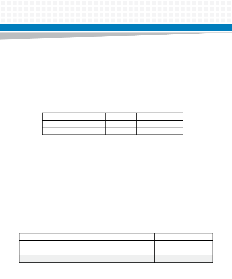
Table 5-3 NAND Flash Map
Start Address
End Address
Size
Description
0000 0000
00FF FFFF
16 MB
Not Used
0100 0000
3FFF FFFF
1 GB - 16 MB
NAND FLASH JFFS2 rootfs
Table 5-4 CCSR Block Base Address Map
Block Base Address (Hex)
Block
Comments
0x00_0000
Local access control—Local configuration control
-
Local access control—Local access windows
-
0x00_1000–0x00_7FFF
Reserved
-