6 boot up options, Table 4-3, Serdes clock configuration by gpio – Artesyn COMX-P4080 Installation and Use (August 2014) User Manual
Page 60: Table 4-4, Rcw source location, Functional description
Functional Description
COMX-P4080 COM Express Module Installation and Use (6806800L20C)
60
It can also be set by three GPIOs.
The setting of the S1 or GPIO depends on the protocols running at the SerDes lanes that belong
to each bank. When the SerDes lanes are running at 3.125 Gbps, the corresponding bank
reference clock should be set as 125 MHz. Any speed other than 3.125 Gbps should be set to
100 MHz. For example, if the lanes in bank 1 are configured as PCI-E, then the bank 1 reference
clock should be set to 100 MHz. If it is set to XAUI, it should be at 125 MHz.
4.6
Boot Up Options
The COMX-P4080 supports several kinds of devices to load configuration information to the
Reset Configuration Word (RCW) register, as well as devices in assisting the U-Boot codes to
boot up the system. This includes NOR flash and NAND flash (both attached to the local bus),
I2C, EEPROM, SPI flash and hardware strapping. The boot option is set by an 8-bit S2 switch. For
more information, see the following table.
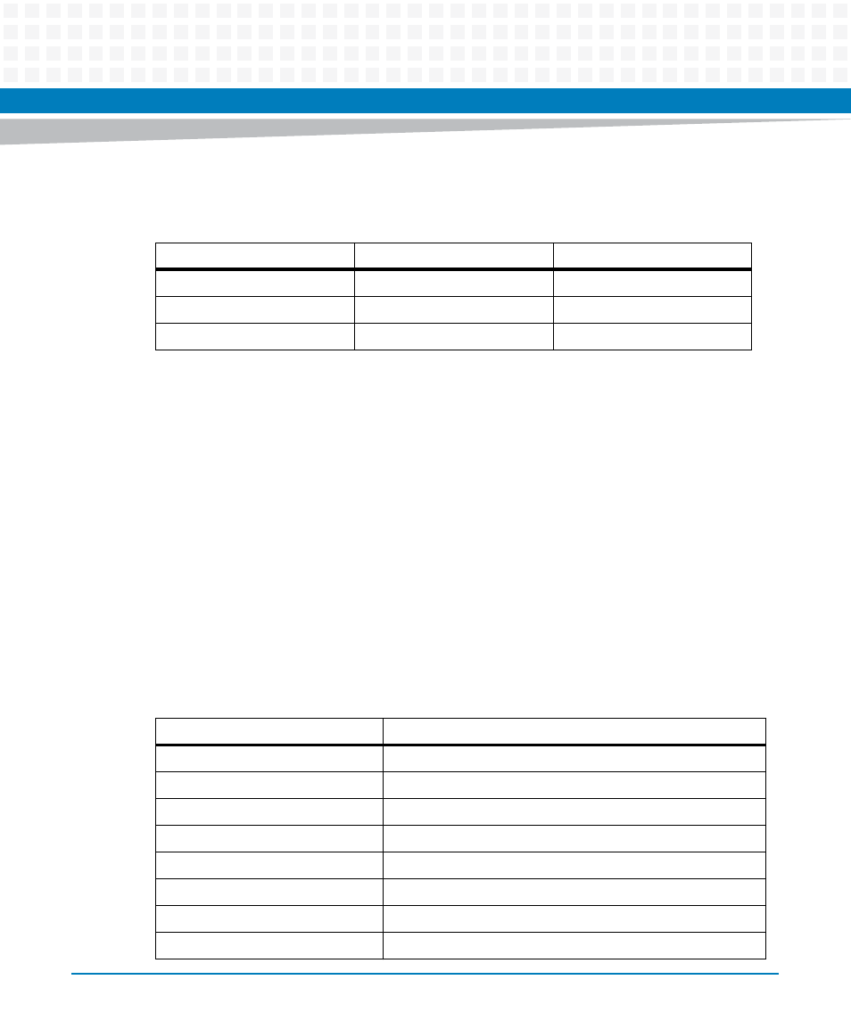
Table 4-3 SerDes Clock Configuration by GPIO
SerDes Bank 1 Reference Clock SerDes Bank 2 Reference Clock SerDes Bank 3 Reference Clock
CPU_GPIO23=0, 100MHz
CPU_GPIO24=0, 100MHz
CPU_GPIO26=0, 100MHz
CPU_GPIO23=1, 125MHz
CPU_GPIO24=1, 125MHz
CPU_GPIO26=1, 125MHz
Default:100MHz
Default:125MHz
Default:125MHz
Table 4-4 RCW Source Location
S2.1 to S2.5
RCW Source
OFF,ON,ON,OFF,ON
I2C1 normal addressing (supports ROMs up to 256 Bytes)
OFF,ON,ON,OFF,OFF
I2C1 extended addressing
OFF,ON,OFF,OFF,ON
SPI 16-bit addressing
OFF,ON,OFF,OFF,OFF
SPI 24-bit addressing
OFF,OFF,ON,OFF,ON
eLBC FCM (NAND flash, 8-bit small page)
OFF,OFF,ON,OFF,OFF
eLBC FCM (NAND flash, 8-bit large page)
OFF,OFF,OFF,OFF,OFF (Default)
eLBC GPCM (NOR flash, 16-bit)
ON,X,X,X,X
Hard-coded RCW options