CIRCUTOR computer PLUS-TF Series User Manual
Page 67
67
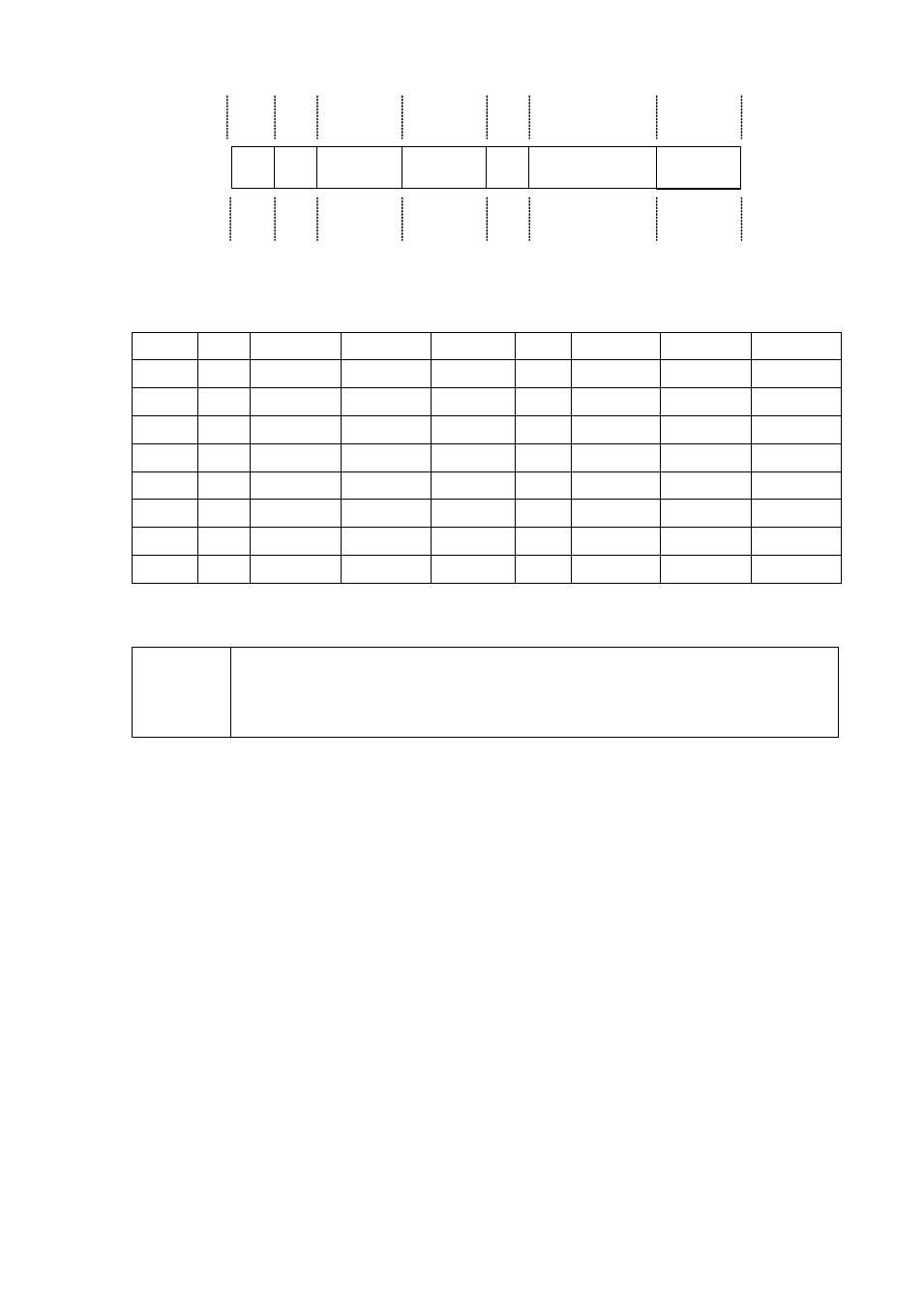
Slave Nr
1 byte
Funct
1 byte
1st bit addr.
2 bytes
Nr of bits
2 bytes
Nr Oct
1 byte
Data
CRC
2 bytes
00
0F
00 - 64
00 - 40
08
DD0 A DD7
XX - XX
Broad,
to all
Funct
15
64 bits
8 octets
Data
8 bytes
CRC
2 bytes
address
Fig. 123.- Control frame of the CPC3i card (MODBUS, function 15)
The meaning of 8 octets DD0 to DD7 is described in table 13-2.
Byte
7 bits 6 bits
5 bits
4 bits
3 bits
2 bits
1 bits
0 bits
DD
0
-
thy3_np2
thy2_np2
thy1_np2
-
thy3_np1
thy2_np1
thy1_np1
DD
1
-
thy3_np4
thy2_np4
thy1_np4
-
thy3_np3
thy2_np3
thy1_np3
DD
2
-
thy3_np6
thy2_np6
thy1_np6
-
thy3_np5
thy2_np5
thy1_np5
DD
3
-
thy3_np8
thy2_np8
thy1_np8
-
thy3_np7
thy2_np7
thy1_np7
DD
4
-
thy3_np10
thy2_np10
thy1_np10
-
thy3_np9
thy2_np9
thy1_np9
DD
5
-
thy3_np12
thy2_np12
thy1_np12
-
thy3_np11
thy2_np11
thy1_np11
DD
6
-
thy3_np14
thy2_np14
thy1_np14
-
thy3_np13
thy2_np13
thy1_np13
DD
7
-
thy3_np16
thy2_np16
thy1_np16
-
thy3_np15
thy2_np15
thy1_np15
Table 13-2.- Meaning of the 8 control bytes
where:
thyn_npx
Thyristor n of the block or peripheral x (This number of peripheral, x, is the one
programmed in the rotating selector for each card).
The frame asks for the transmission of data to thyristors in up to 16 different steps,
phase by phase