Power measurement – Altera Transceiver Signal Integrity Development Kit, Stratix V GX Edition User Manual
Page 55
Appendix A: Board Revision History
A–3
Engineering Silicon Version Differences
July 2012
Altera Corporation
Transceiver Signal Integrity Development Kit
Stratix V GX Edition Reference Manual
Power Measurement
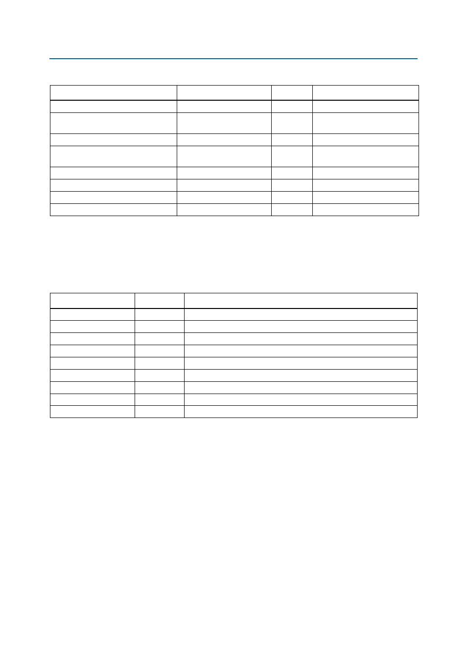
Table A–3
lists information for the voltage rails whose values on the engineering
silicon board differ from the production silicon board.
the production silicon voltage values.
Temperature sense ADC
3p3V
3.3
—
ICS557-03 spread spectrum clock buffer
(x1)
3p3V
3.3
25-MHz clock output to the FPGA
ICS8304 clock buffer
3p3V/2p5V
3.3/2.5
50-MHz clock outputs
IDT5T9306 transceiver REFCLK clock
buffers (x4)
2p5V
2.5
Programmable clock outputs
T85A23157 dual analog switch
5V
5.0
—
Character LCD
5V
5.0
—
LEDs (x13)
2p5V
2.5
—
Board power LED
5V
5.0
—
Table A–2. Power Requirements (Engineering Silicon)
Device
Voltage Name
Voltage (V)
Note
Table A–3. Voltage Rails (Engineering Silicon)
Schematic Net Name
Voltage (V)
Description
S5GX_VCC
0.9
VCC, VCCHIP, VCCHSSI FPGA core power.
VCCR_GTB
1.1
Transceiver receiver power for 28G channels.
VCCT_GTB
1.1
Transceiver transmit power for 28G channels.
VCCL_GTB
1.1
Transceiver clocking power for 28G channels.
VCCRT_GXB
1.0 or 1.2
Shared VCCR_GXB and VCCT_GXB transceiver power for 12.5G channels.
VCCA_GXB
2.5 or 3.3
Transceiver analog clock power
VCCH_GXB
1.6
Transceiver TX buffer voltage
VCCD_PLL
1.6
FPGA core D PPL voltage
VCCPT
1.6
FPGA programmable power technology