Altera Transceiver Signal Integrity Development Kit, Stratix V GX Edition User Manual
Page 20
2–12
Chapter 2: Board Components
MAX II CPLD System Controller
Transceiver Signal Integrity Development Kit
July 2012
Altera Corporation
Stratix V GX Edition Reference Manual
MAXLL_BEN0
F5
AN15
2.5-V
Flash bus MAX II byte enable 0
MAXLL_BEN1
F2
AN14
2.5-V
Flash bus MAX II byte enable 1
MAXLL_BEN2
F6
AM14
2.5-V
Flash bus MAX II byte enable 2
MAXLL_BEN3
F1
AR14
2.5-V
Flash bus MAX II byte enable 3
MAXLL_CLK
G3
AR13
2.5-V
Flash bus MAX II clock
MAXLL_CSn
G2
AR15
2.5-V
Flash bus MAX II chip select
MAXLL_OEn
G4
AP15
2.5-V
Flash bus MAX II output enable
MAXLL_WEn
G1
AT15
2.5-V
Flash bus MAX II write enable
MSEL0
D13
W12
2.5-V
DIP - FPGA mode select 0
MSEL1
K12
Y11
2.5-V
DIP - FPGA mode select 1
MSEL2
K13
AA12
2.5-V
DIP - FPGA mode select 2
MSEL3
L11
AA11
2.5-V
DIP - FPGA mode select 3
MSEL4
L12
W11
2.5-V
DIP - FPGA mode select 4
NCONFIG
R14
U26
2.5-V
FPGA configuration active LED
NSTATUS
R12
AL10
2.5-V
FPGA configuration ready status LED
OVERTEMPn
E4
E7
2.5-V
Temperature monitor over-temperature indicator LED
PFL_STATUS
P4
—
2.5-V
Parallel Flash Loader (PFL) programming status
PGM0
T6
AW10
2.5-V
Flash memory PGM select indicator 0
PGM1
T5
AV10
2.5-V
Flash memory PGM select indicator 1
PGM2
T4
AR12
2.5-V
Flash memory PGM select indicator 2
PGMSEL
T7
—
2.5-V
Toggles the PGM_LED[0:2] sequence
PM1_FAULTB00
C4
U14
2.5-V
Power monitor bus
PM1_FAULTB01
C6
U13
2.5-V
Power monitor bus
PM1_FAULTB10
B3
R12
2.5-V
Power monitor bus
PM1_FAULTB11
C5
P11
2.5-V
Power monitor bus
PM2_FAULTB00
A2
N13
2.5-V
Power monitor bus
PM2_FAULTB01
D5
N12
2.5-V
Power monitor bus
PM2_FAULTB10
B1
R13
2.5-V
Power monitor bus
PM2_FAULTB11
D4
P13
2.5-V
Power monitor bus
PM_ALERTB
B4
L12
2.5-V
Power monitor alert
PM_CNTL0
C7
K12
2.5-V
Power monitor control bus
PM_CNTL1
A4
K13
2.5-V
Power monitor control bus
PM_PWRGD
D6
V12
2.5-V
Power monitor power
PM_RSTN
E6
J13
2.5-V
Power monitor reset
PM_SHARE_CLK
B5
M12
2.5-V
Power monitor clock
PR_DONE
B6
AB29
2.5-V
FPGA partial reconfiguration done
PR_ERROR
D7
AC27
2.5-V
FPGA partial reconfiguration error
PR_READY
A5
AD29
2.5-V
FPGA partial reconfiguration ready
PR_REQUEST
E7
AE29
2.5-V
FPGA partial reconfiguration request
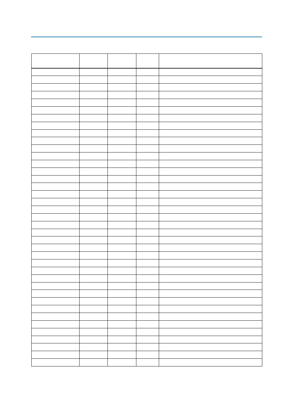
Table 2–5. MAX II CPLD System Controller Device Pin-Out (Part 4 of 5)
Schematic Signal
Name
MAX II CPLD
Pin Number
Stratix V GX
Pin Number
i/O
Standard
Description