Fpga programming over external usb-blaster, Jtag header – Altera Transceiver Signal Integrity Development Kit, Stratix V GX Edition User Manual
Page 25
Chapter 2: Board Components
2–17
Configuration, Status, and Setup Elements
July 2012
Altera Corporation
Transceiver Signal Integrity Development Kit
Stratix V GX Edition Reference Manual
f
For more information on the Nios II processor, refe
page of
the Altera website.
FPGA Programming over External USB-Blaster
The JTAG header provides another method for configuring the FPGA (U29) using an
external USB-Blaster device with the Quartus II Programmer running on a PC. The
external USB-Blaster is connected to the board through the JTAG header (J93). The
JTAG DIP switch (S7) allows the MAX II CPLD device to be removed from the JTAG
chain so that the FPGA is the only device on the JTAG chain.
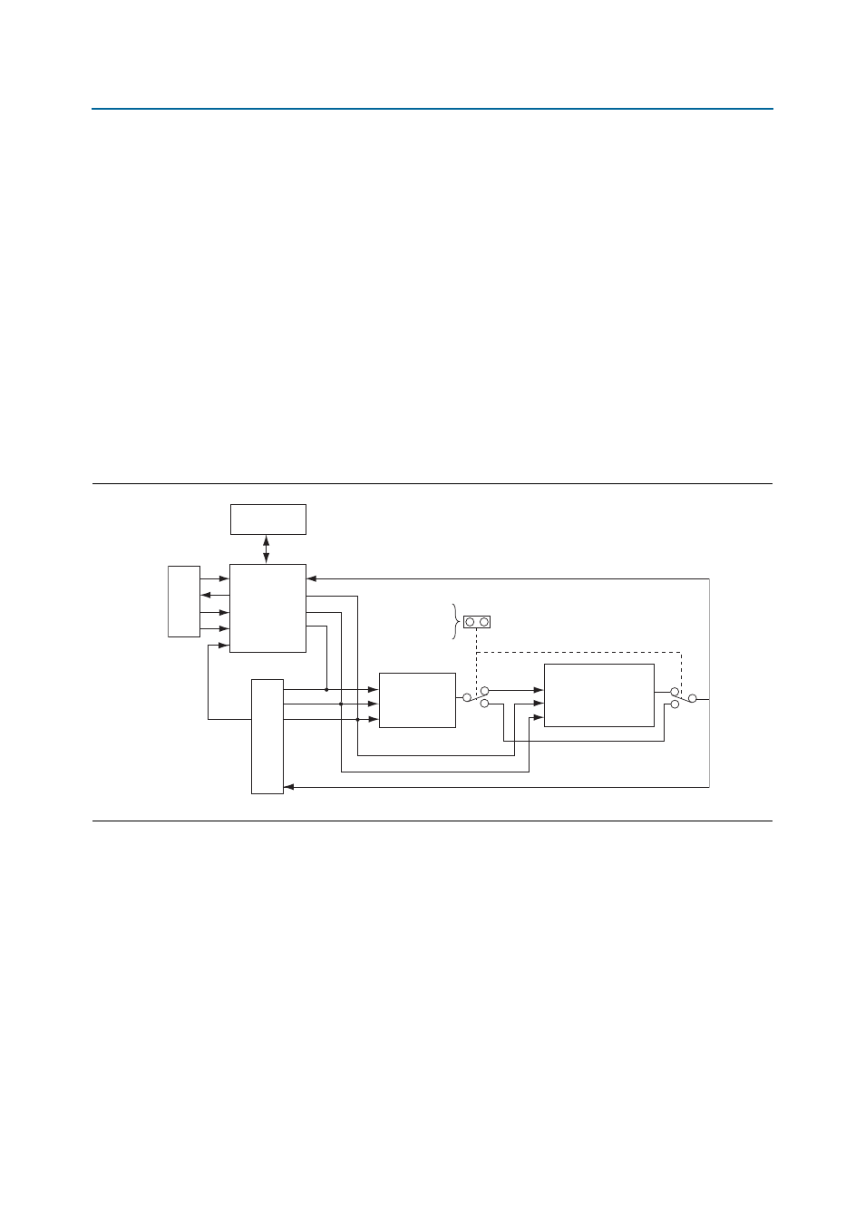
JTAG Header
The JTAG header provides another method for configuring the FPGA using an Altera
USB-Blaster dongle with the Quartus II Programmer running on a PC.
shows the schematic connections for the dedicated JTAG programming header (J93).
The program MSEL switch (S7) allows the MAX II CPLD device to be removed from
the JTAG chain so that the FPGA is the only device on the JTAG chain.
The MAX II CPLD System Controller must be in the chain to use some of the GUI
interfaces. For this setting, set pins 6-7 of the program MSEL switch (S7) to 1.
f
For more information on the following topics, refer to the respective documents:
■
Board Update Portal and PFL Design, refer to the
■
PFL megafunction, refer to
Figure 2–5. JTAG Header
Stratix V GX FPGA
External USB-Blaster Header
Remove jumper to exclude
the MAX CPLD device
from the JTAG chain.
Jumper
Dual
Analog
Switch
TDI
TMS
TCK
LAST_TDO
LAST_TDO
S5GX_TDI
S5GX_TDO
JTAG_TMS
JTAG_TCK
MAX CPLD
TDI
TDO
TMS
TCK
IO_TDI
IO_TDO
IO_TMS
IO_TCK
MAX_OEn
JTAG_TMS
JTAG_TCK
MAX_FPP_TDI MAX_FPP_TDO
MAX II and Flash FPP
9
5
1
2
3
JTAG
Header
USB Interface
9
5
1
3