Power measurement, Power measurement –65 – Altera Stratix IV GX FPGA Development Board User Manual
Page 73
Chapter 2: Board Components
2–65
Power Supply
November 2010
Altera Corporation
Stratix IV GX FPGA Development Board, 530 Edition Reference Manual
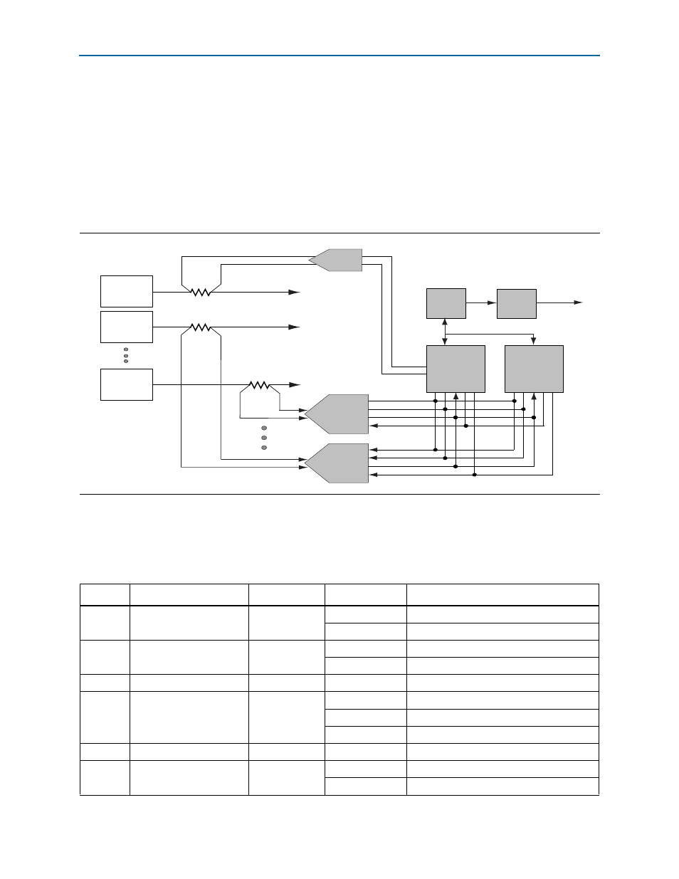
Power Measurement
There are 16 power supply rails which have on-board voltage and current sense
capabilities. These 8-channel differential 24-bit ADC devices and rails are split from
the primary supply plane by a low-value sense resistor for the ADC to measure
voltage and current. A serial peripheral interface (SPI) bus connects these ADC
devices to the MAX II CPLD EPM2210 System Controller as well as the Stratix IV GX
FPGA.
Figure 2–16
shows the block diagram for the power measurement circuitry.
lists the targeted rails. The schematic signal name specifies the name of the
rail being measured and the device pin specifies the devices attached to the rail. If no
subnet is named, the power is the total output power for that voltage.
Figure 2–16. Power Measurement Circuit
SCK
DSI
DSO
CSn
8 Ch.
To Plane 0x0
To Plane 0xE
Supply
0x0
Supply
0xE
R
SENSE
R
SENSE
SCK
DSI
DSO
CSn
8 Ch.
EPM2210
EP4SGX530
LTC2418
LTC2418
U1
EPM
240
USB
PHY
To User PC
Power GUI
JTAG Chain
SPI Bus
Embedded
USB-Blaster
To Plane 0xF
12 V
Supply
R
SENSE
SCL
SDA
1 Ch.
LTC4151
SM Bus
U9
U36
Table 2–58. Power Rail Measurements Based on the Rotary Switch Position (Part 1 of 2)
Switch
Schematic Signal Name
Voltage (V)
Device Pin
Description
0
S4VCCIO_B7B8
1.5
VCCIO_B7
Bank 7 I/O power (QDR2TOP+DDR3TOP)
VCCIO_B8
Bank 8 I/O power (QDR2TOP+DDR3TOP)
1
S4VCC
0.9
VCC
FPGA core and periphery power
VCCHIP
PCI Express hard IP block
2
3.3 V
3.3
—
All 3.3 V power to board (mA only)
3
S4VCCIO_INT
2.5
VCCPD
I/O pre-drivers
VCCPGM
Configuration I/O
VCC_CLKIN
V
IO
clock input pins
4
S4VCCH_GXB
1.4
VCCH_GXB
XCVR clock buffers
5
S4VCCAUX
2.5
VCCAUX
Programmable power tech auxiliary
VCCA_PLL
PLL analog