Power supply, Power supply –63 – Altera Stratix IV GX FPGA Development Board User Manual
Page 71
Chapter 2: Board Components
2–63
Power Supply
November 2010
Altera Corporation
Stratix IV GX FPGA Development Board, 530 Edition Reference Manual
lists the flash memory component reference and manufacturing
information.
Power Supply
The development board’s power is provided through a laptop style DC power input.
The input voltage must be in the range of 14 V to 20 V. The DC voltage is then stepped
down to the various power rails used by the components on the board and installed
into the HSMC connectors.
An on-board multi-channel analog-to-digital converter (ADC) is used to measure both
the voltage and current for several specific board rails. The power utilization is
displayed in a GUI that graphs power consumption versus time.
U32.F6
Address valid
FLASH_ADVn
2.5-V
AN31
U32.F7
Ready
FLASH_RDYBSYn
AT32
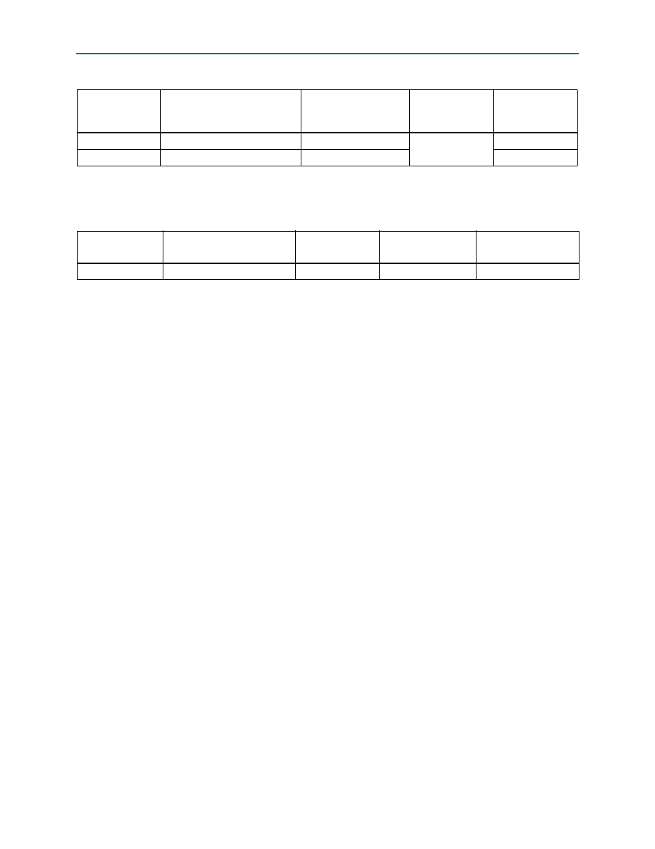
Table 2–56. Flash Pin Assignments, Schematic Signal Names, and Functions (Part 3 of 3)
Board Reference
Description
Schematic Signal Name
I/O Standard
Stratix IV GX
Device
Pin Number
Table 2–57. Flash Memory Component Reference and Manufacturing Information
Board Reference
Description
Manufacturer
Manufacturing
Part Number
Manufacturer
Website
U32
512-Mbyte synchronous flash
Numonyx
PC28F512P30BF