Development board block diagram, Development board block diagram –2, Sdi –2 – Altera SDI HSMC User Manual
Page 6
1–2
Chapter 1: Overview
Board Component Blocks
© July 2009 Altera Corporation
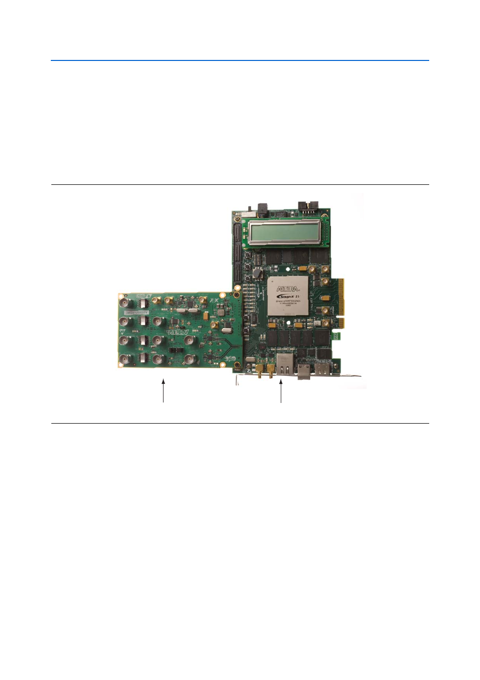
shows the SDI HSMC connected to an Altera FPGA development board.
f
for an
example of connecting the SDI HSMC to a host board.
f
For detailed information about the board components and interfaces of the Stratix IV
GX FPGA development board, refer to the
.
Development Board Block Diagram
shows the functional block diagram of the SDI HSMC. The board has three
distinct areas of interest:
■
SDI
■
AES
■
Clocking
SDI
The SDI includes two high-speed output interfaces from the HSMC to the cable
drivers and to two single-ended 75-
Ω BNC output interfaces. There are also two
receive paths which input signals to two 75-
Ω BNC connectors to receive equalizers.
The differential signals are then output to the HSMC connector.
Figure 1–1. SDI HSMC Connected to the Stratix IV GX FPGA Development Board
SDI HSMC
Stratix IV GX FPGA Development Board
- MAX 10 JTAG (15 pages)
- MAX 10 Power (21 pages)
- Unique Chip ID (12 pages)
- Remote Update IP Core (43 pages)
- Device-Specific Power Delivery Network (28 pages)
- Device-Specific Power Delivery Network (32 pages)
- Hybrid Memory Cube Controller (69 pages)
- ALTDQ_DQS IP (117 pages)
- MAX 10 Embedded Memory (71 pages)
- MAX 10 Embedded Multipliers (37 pages)
- MAX 10 Clocking and PLL (86 pages)
- MAX 10 FPGA (26 pages)
- MAX 10 FPGA (56 pages)
- USB-Blaster II (22 pages)
- GPIO (22 pages)
- LVDS SERDES (27 pages)
- User Flash Memory (33 pages)
- ALTDQ_DQS2 (100 pages)
- Avalon Tri-State Conduit Components (18 pages)
- Cyclone V Avalon-MM (166 pages)
- Cyclone III FPGA Starter Kit (36 pages)
- Cyclone V Avalon-ST (248 pages)
- Stratix V Avalon-ST (286 pages)
- Stratix V Avalon-ST (293 pages)
- DDR3 SDRAM High-Performance Controller and ALTMEMPHY IP (10 pages)
- Arria 10 Avalon-ST (275 pages)
- Avalon Verification IP Suite (224 pages)
- Avalon Verification IP Suite (178 pages)
- FFT MegaCore Function (50 pages)
- DDR2 SDRAM High-Performance Controllers and ALTMEMPHY IP (140 pages)
- Floating-Point (157 pages)
- Integer Arithmetic IP (157 pages)
- Embedded Peripherals IP (336 pages)
- JESD204B IP (158 pages)
- Low Latency Ethernet 10G MAC (109 pages)
- LVDS SERDES Transmitter / Receiver (72 pages)
- Nios II Embedded Evaluation Kit Cyclone III Edition (3 pages)
- Nios II Embedded Evaluation Kit Cyclone III Edition (80 pages)
- IP Compiler for PCI Express (372 pages)
- Parallel Flash Loader IP (57 pages)
- Nios II C2H Compiler (138 pages)
- RAM-Based Shift Register (26 pages)
- RAM Initializer (36 pages)
- Phase-Locked Loop Reconfiguration IP Core (51 pages)
- DCFIFO (28 pages)