Altera SDI HSMC User Manual
Page 16
2–8
Chapter 2: Board Components
Clock Circuitry
© July 2009 Altera Corporation
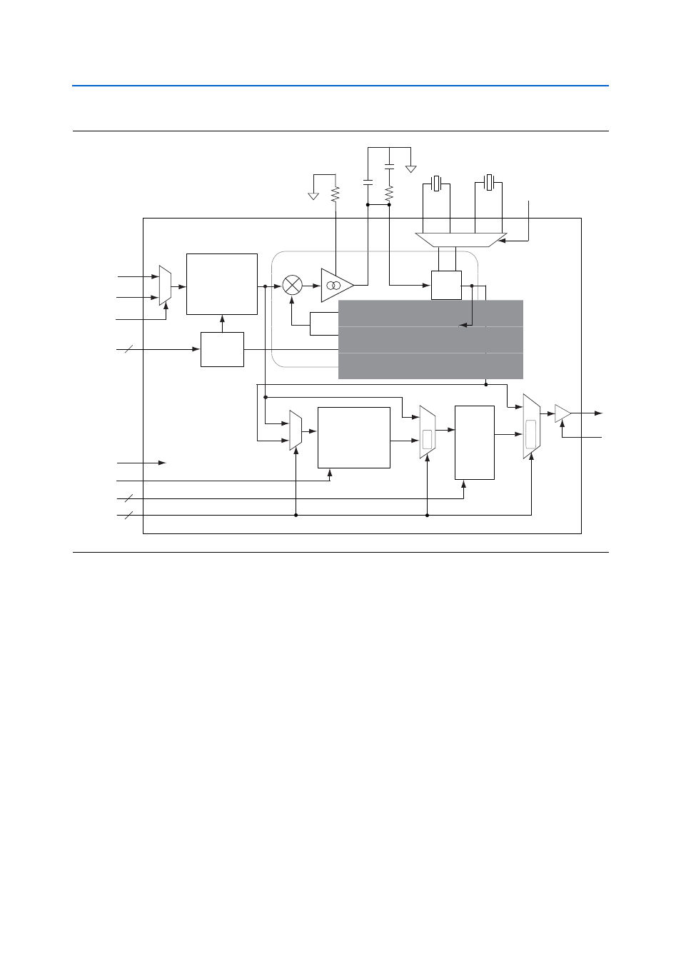
The clock control signals SDI_CLK_V[3:0] control the input divider for the first
translation stage of the SDI multi-frequency VCXO femto clock video PLL.
shows which frequency inputs lock to either 27 MHz or 26.973027 MHz crystals.
Various "P" and "M" preset divider options can be selected by adjusting the values to
produce a frequency of 27 MHz or the alternate frequency out of the VCXO. The "P"
divider divides the input frequency to the comparison frequency used by the phase
detector. The "M" divider divides the output frequency of the VCXO to the
comparison frequency used by the phase detector. After the VCXO is locked to
27 MHz (or alternate), the signal is then multiplied up to the output frequency by the
femto clock PLL (refer to
). The output frequency can be 148.5 MHz,
74.25 MHz, 54 MHz, or 36 MHz. The output frequency is set to 148.5 MHz for the
Altera reference design and most applications.
lists the first frequency translation stage of the SDI multi-frequency VCXO
femto clock video PLL.
Figure 2–4. SDI Multi-Frequency VCXO Femto Clock Video PLL Block Diagram
Output
Divider
00 = 4
01 = 8
10 = 12
11 = 18
SDI CLK
VCXO Input
Pre-divider
(P Value from
Table 2-6)
2
2
4
VCXO Feedback Divider
(M Value from Table)
0
1
Femto Clock
Frequency Multiplier
0 = x22
1 = x24
VCXO PLL
Divider
Look-up Table
VCXO
0
1
01
10
11
00
01
10
11
0
1
+
–
CLK0
CLK1
CLK_SEL
V3:V0
MR
Master Reset
MF
N1:N0
nBP1:nBP0
Phase
Detector
Charge
Pump
ISET
LF0
Loop
Filter
LF1
XTAL_IN0
XTAL_OUT0
XTAL_IN1
XTAL_OUT1
XTAL_SEL