Altera SDI HSMC User Manual
Page 11
Chapter 2: Board Components
2–3
Board Overview
© July 2009 Altera Corporation
describes the components and lists their corresponding board references.
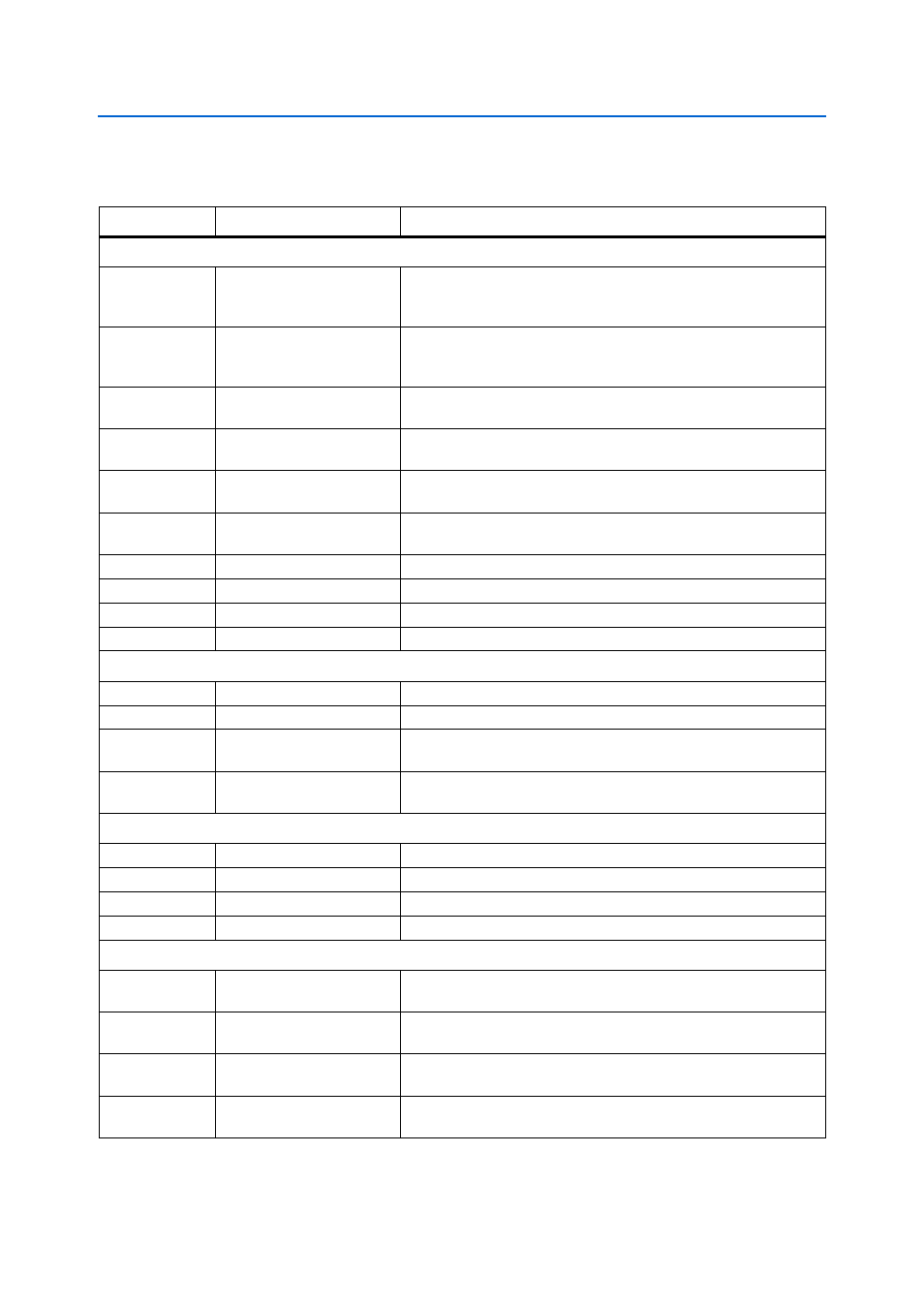
Table 2–1. SDI HSMC Components (Part 1 of 2)
Board Reference
Name
Description
Devices
U1, U2
SDI cable tri-speed driver
Input signal to this driver is from the HSMC high-speed
serializer/deserializer (SERDES) section. The DC blocking caps are in
series with the connector and the integrated circuit (IC).
U3
AES VCXO PLL
Programmed VCXO from Integrated Computer Solutions (ICS) to
produce frequencies of 98.304 MHz, 90.3168 MHz, 122.88 MHz, and
112.896 MHz.
U4
Multi-format video sync
separator
Signals ODDEVEN, VFORMAT, VSYNC, HSYNC from this device are
available to the host board through the HSMC connector.
U5
High frequency switching
regulator
IC switching power supply configured for a 5 V output. The input
voltage is 12 V from the HSMC connector.
U6
SDI multi-frequency VCXO
femto clock video PLL
Low jitter femto clock, multi-crystal SDI video PLL.
U7
LVPECL differential clock
buffer
Differential clock signals available at the SMA outputs and HSMC
connector.
U8, U10
SDI cable equalizer
Equalizes data transmitted over the cable.
U9, U16
RS422 transceiver
Used as a differential line driver and receiver for the AES interface.
U11, U12, U13
Linear regulator
Regulator with an input of 5 V and output of 3.3 V.
U14, U15
Single gate tri-state buffer
For AES VCXO control.
SDI Inputs/Outputs
J1
SDI output channel 2
Output is through a BNC connector driven from the SDI cable driver.
J8
SDI output channel 1
Output is through a BNC connector driven from the SDI cable driver.
J2
SDI input channel 2
The signal from this channel is input to a cable equalizer. This equalizer
can be bypassed.
J9
SDI input channel 1
The signal from this channel is input to a cable equalizer. This equalizer
can be bypassed.
AES Inputs/Outputs
J3
AES output channel 1
Transformer-coupled output with 75-
Ω driver impedance.
J10
AES input channel 1
A 75-
Ω transformer coupled with AES input channel.
J14
AES output channel 2
Transformer-coupled output with 75-
Ω driver impedance.
J15
AES input channel 2
A 75-
Ω transformer coupled with AES input channel.
Clocks
J16
SMA SDI clock input
This signal is input to the SDI clock PLL (CMOS). There is a 49.9-
Ω
termination to ground at the pin.
J17
SMA SDI clock output (P)
An ECL compatible output. The ECL bias includes a 130-
Ω pull-up to
3.3 V and a 82-
Ω pull-down to ground.
J18
SMA SDI clock output (N)
An ECL compatible output. The ECL bias includes a 130-
Ω pull-up to
3.3 V and a 82-
Ω pull-down to ground.
J12
SMA AES clock output
This signal is output to the SMA AES clock (CMOS) and has a 33-
Ω
series termination resistor.