Supported protocols, Supported protocols –4 – Altera SDI HSMC User Manual
Page 12
2–4
Chapter 2: Board Components
Supported Protocols
© July 2009 Altera Corporation
Supported Protocols
lists the SDI video standards supported by the SDI HSMC.
General User Input/Output
J7
SDI input 1 equalizer bypass
jumper
Installing a jumper on J7 enables the LMH0344 device's equalization
and DC restoration features for channel 1. Removing a jumper from J7
bypasses the equalizer (default). This can also be controlled by driving
EQ_BYPASS1
low from the HSMC host board through connector J19
pin 77. Remove the jumper when controlling from the HSMC host
board's FPGA.
J5
SDI input 2 equalizer bypass
jumper
Installing a jumper on J5 enables the LMH0344 device's equalization
and DC restoration features for channel 2. Removing a jumper from J5
bypasses the equalizer (default). This can also be controlled by driving
EQ_BYPASS2
low from the HSMC host board through connector J19
pin 79. Remove the jumper when controlling from the HSMC host
board's FPGA.
J6
SDI input 1 auto-mute enable
jumper
Installing a jumper on J6 enables the LMH0344 device's carrier detect
function to auto-mute its own output when no input signal is detected
from J9 for channel 1. Removing a jumper from J6 causes the mute
function to be enabled. Altera recommends to leave this jumper
installed.
J4
SDI input 2 auto-mute enable
jumper
Installing a jumper on J4 enables the LMH0344 device's carrier detect
function to auto-mute its own output when no input signal is detected
from J2 for channel 2. Removing a jumper from J4 may cause the mute
function to be enabled. Altera recommends to leave this jumper
installed.
Components and Interfaces
J19
HSMC connector
SDI HSMC’s main interface to the host board. The host must support
3-Gbps interfacing on transceiver channels 0 and 1 (first 2 channels)
which are located at pins 25 – 32. The control, clock, and AES signals
are located in the general CMOS signal area. The AES clock is
single-ended while the SDI clock is differential.
Power
J19
HSMC 12-V input
12-V input from the HSMC connector is utilized for board power
generation. Power of 5 V is produced by a low noise high frequency
switcher. Three linear regulators are used to produce 3.3 V from the 5-V
power rail.
Table 2–1. SDI HSMC Components (Part 2 of 2)
Board Reference
Name
Description
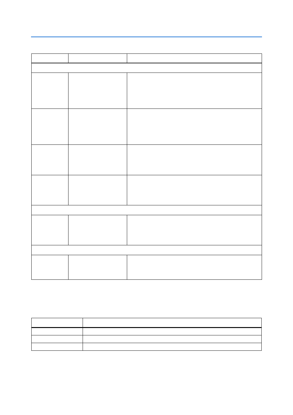
Table 2–2. SDI supported protocols
Rate
Video Standard
Standard Definition (SD)
NTSC, PAL
High Definition (HD)
720p50, 720p59, 720p60, 1080s23.98, 1080s24, 1080i50, 1080i60, 1080p29.97, 1080p30
Third-Generation (3G)
1080p50, 1080p59.9, 1080p60