Host board reference clock –10, Table 2–7 – Altera SDI HSMC User Manual
Page 18
2–10
Chapter 2: Board Components
Clock Circuitry
© July 2009 Altera Corporation
1
are mainly used for testing. For normal operation,
the nBP signals are both driven to logic 1.
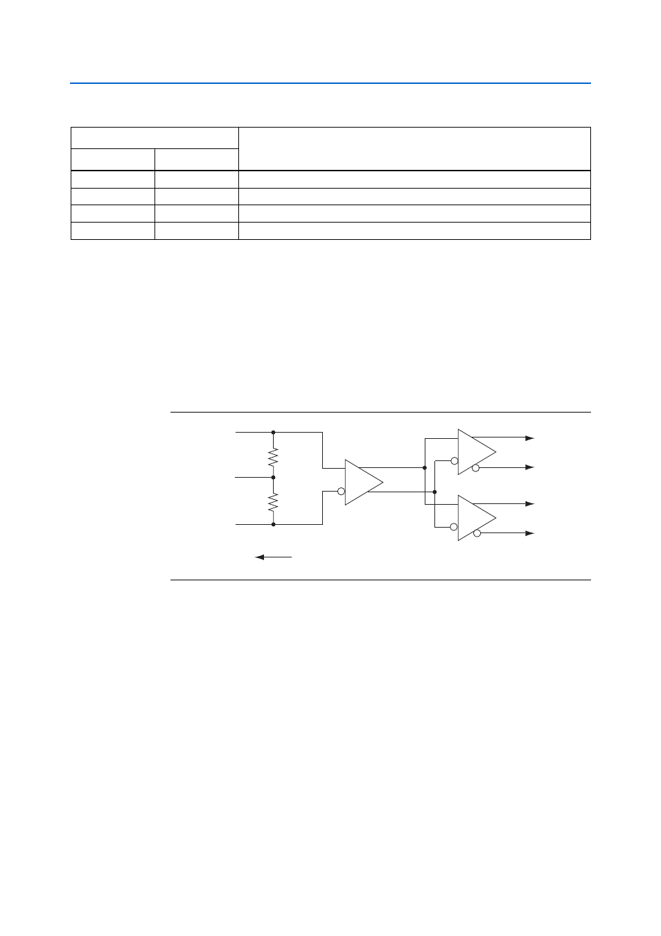
The output of the clock generator is single-ended. To avoid common mode noise that
might be present in the signaling path from the clock generator to the HSMC host
device, a differential LVPECL clock buffer is employed to convert the reference clock
to differential signal and drive the signal to the host device. The LVPECL differential
clock buffer (SY58012) has the advantages of a fast edge rate and low jitter.
shows a simplified block diagram of the LVPECL differential clock buffer.
The differential outputs at Q0 are connected to the HSMC connector and drive the
clock signal to the host device. The outputs at Q1 have output bias resistors and are
connected to two 50-
Ω SMA connectors. These outputs serve as a low jitter source to
sync up other system devices and to trigger on test equipment or alternate reference
clock source to the host board.
Host Board Reference Clock
You can select one of the several reference clock frequencies to input as a reference to
the SDI multi-frequency VCXO femto clock video PLL. For example, if the host board
has a 100-MHz oscillator, you can divide the frequency by 6,400 to 15.625 kHz and
drive that frequency to the clock generator to be multiplied to 148.5 MHz. Altera
recommends locking the VCXO PLL to a stable oscillator which is located on the host
board when the daughtercard is sourcing data or when the VCXO PLL is not locked
onto a received signal or reference. This locking prevents wandering or frequency
hunting.
Table 2–7. Bypass Function Table
Inputs
Operation
nBP1
nBP0
0
0
Bypass frequency translator PLL and output divider.
0
1
Test mode: Bypass VCXO jitter attenuation PLL and frequency translator PLL.
1
0
LC mode: Bypass VCXO jitter attenuation PLL.
1
1
PLL mode: Active.
Figure 2–5. LVPECL Differential Clock Buffer
IN
V
T
/IN
Q0
/Q0
Q1
/Q1
50
Ω
50
Ω
V
REF
– AC