Development board block diagram, Handling the board – Altera Arria II GX FPGA Development Board User Manual
Page 8
1–4
Chapter 1: Overview
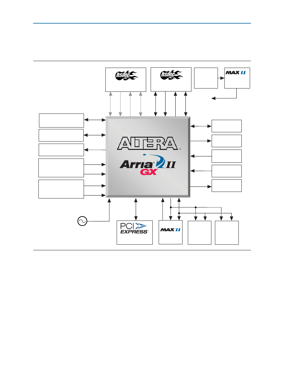
Development Board Block Diagram
Arria II GX FPGA Development Board Reference Manual
February 2011
Altera Corporation
Development Board Block Diagram
shows the block diagram of the Arria II GX FPGA development board.
Handling the Board
When handling the board, it is important to observe the following precaution:
c
Without proper anti-static handling, the board can be damaged. Therefore, use
anti-static handling precautions when touching the board.
c
In order to avoid damaging the board due to voltage spikes, place the power switch
(SW1) in the OFF position prior to plugging in the DC Input power jack.
Figure 1–1. Arria II GX FPGA Development Board Block Diagram
Port B*
Port A
128 Mbyte
DDR3 (x16)
2x16 LCD
Push-button
Switches
DIP Switch
LEDs
CPLD
64 Mbyte
Flash
2 Mbyte
SSRAM
x8 Edge
1 Gbyte
DDR2 SODIMM (x64)
Gigabit Ethernet
PHY (RGMII)
Clock SMA OUT
Programmable Oscillator
100 M, 125 M, 156.25 M,
SMA (LVPECL)
Embedded
Blaster
USB
2.0
x120
x16
x1
x1 CLK IN
x1 REF CLK
x50
x11
x3
x4
x26 ADDR
XCVR x8
x8 Config
x76
CLKIN x2
CLKOUT x2
XCVR x4
x74
CLKIN x3
CLKOUT x3
XCVR x4
JTAG Chain
Programmable Oscillator
100 M, 125 M, 156.25 M,
x1 CLK IN
x3 REF CLK
x32 DATA
x1 REF CLK
EP2AGX125EF35
Z
Z
x4
155.52 MHz
*Port B is only connected on
EP2AGX260EF35 devices.