Altera Arria II GX FPGA Development Board User Manual
Page 11
Chapter 2: Board Components
2–3
Board Overview
February 2011
Altera Corporation
Arria II GX FPGA Development Board Reference Manual
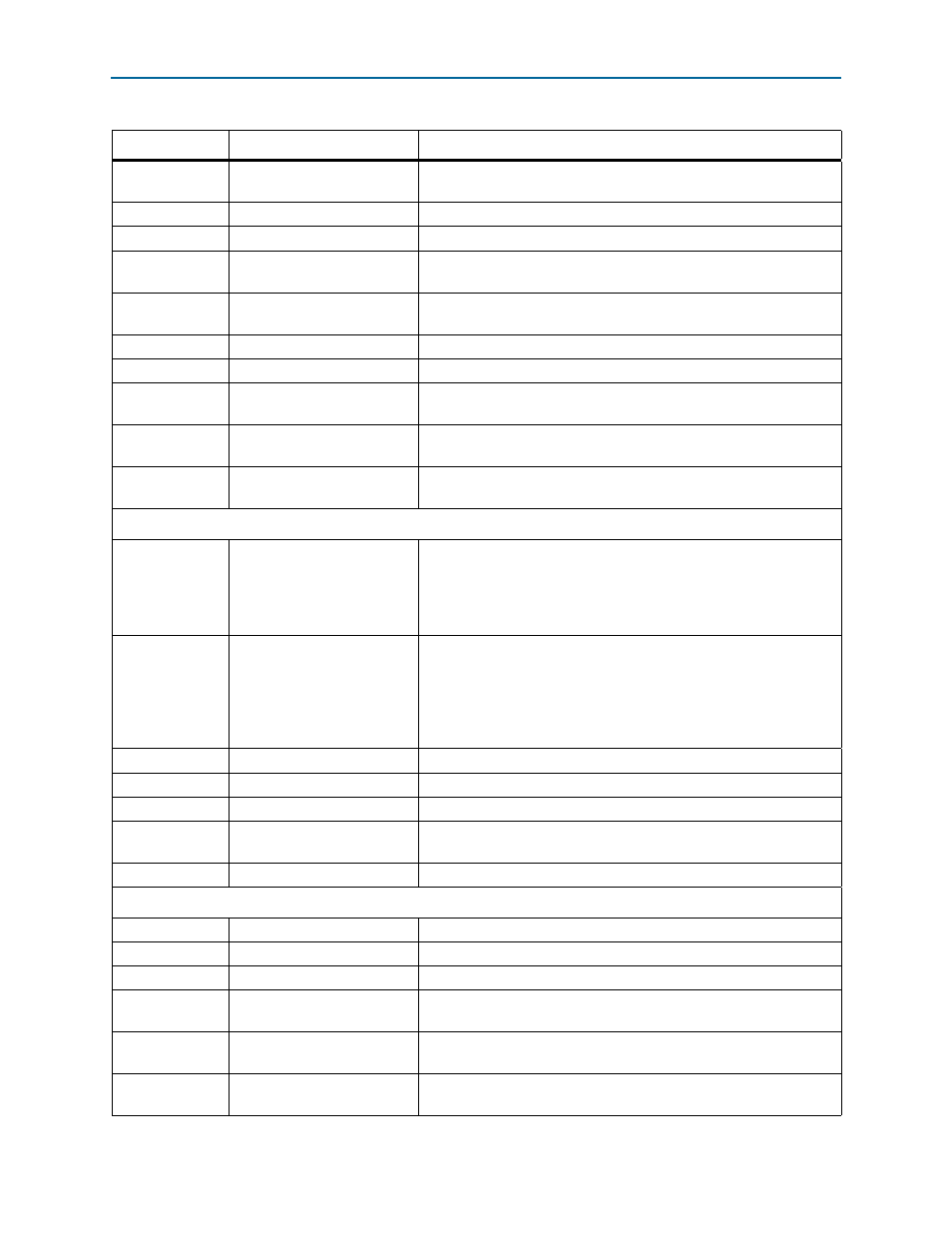
D15
Load LED
Illuminates when the MAX II CPLD EPM2210 System Controller is
actively configuring the FPGA.
D16
Error LED
Illuminates when the FPGA configuration from flash memory fails.
D18
Power LED
Illuminates when 2.5-V power is present.
D11, D12, D13
Configuration LEDs
Illuminates to show the LED sequence that determines which flash
memory image loads to the FPGA when LOAD IMAGE is pressed.
D19, D20, D21,
D22, D23
Ethernet LEDs
Shows the connection speed as well as transmit or receive activity.
D4, D5
HSMC port A LEDs
You can configure these LEDs to indicate transmit or receive activity.
D6
HSMC port A present LED
Illuminates when a daughtercard is plugged into the HSMC port A.
D2, D3
HSMC port B LEDs
You can configure these LEDs to indicate transmit or receive activity
(only populated when a EP2AGX260 device is installed).
D1
HSMC port B present LED
Illuminates when a daughtercard is plugged into the HSMC port B
(only populated when a EP2AGX260 device is installed).
D24, D25, D26
PCI Express link LEDs
You can configure these LEDs to display the PCI Express link width
(x1, x4, x8).
Clock Circuitry
U26
Programmable oscillator
(125 MHz default)
Programmable oscillator with a default frequency of 125.00 MHz. The
frequency is programmable using the MAX II CPLD EPM2210 System
Controller. For general use such as memories, gigabit Ethernet
(125 M/156.25 M), Serial RapidIO™ (SRIO) (125 M), or PCI Express
(100 M).
U30
Programmable oscillator
(100 MHz default)
Programmable oscillator with a default frequency of 100.00 MHz. The
frequency is programmable using the MAX II CPLD EPM2210 System
Controller. For general use such as memories, gigabit Ethernet
(125 M/156.25 M), SRIO (125 M), PCI Express (100 M), or XAUI
(156.25 M). Multiplex with CLKIN_SMA_P based on CLK_SEL switch
value.
Y5
50 MHz oscillator
50.000 MHz crystal oscillator for general purpose logic.
Y6
100 MHz oscillator
100.000 MHz crystal oscillator for general purpose logic.
U25
155.52 MHz oscillator
155.520 MHz crystal oscillator for SONET.
J10, J11
Clock input SMAs
Drive LVPECL-compatible clock inputs into the clock multiplexer buffer
(U33).
J12
Clock output SMA
Drive out 2.5-V CMOS clock output from the FPGA.
General User Input/Output
D7, D8, D9, D10
User LEDs
Four user LEDs. Illuminates when driven low.
SW2
User DIP switch
Quad user DIP switches. When the switch is ON, a logic 0 is selected.
PB3
CPU reset push-button switch
Press to reset the FPGA logic.
PB4
MAX II reset push-button
switch
Press to reset the MAX II CPLD EPM2210 System Controller.
PB1, PB2
General user push-button
switches
Two user push-button switches. Driven low when pressed.
PB6
Image select push-button
switch
Toggles the configuration LEDs which selects the program image that
loads from flash memory to the FPGA.
Table 2–1. Arria II GX FPGA Development Board Components (Part 2 of 3)
Board Reference
Type
Description