Components and interfaces, Pci express, Components and interfaces –28 – Altera Arria II GX FPGA Development Board User Manual
Page 36: Pci express –28

2–28
Chapter 2: Board Components
Components and Interfaces
Arria II GX FPGA Development Board Reference Manual
February 2011
Altera Corporation
1
The particular model used does not have a backlight and the LCD drive pin is not
connected.
f
For more information such as timing, character maps, interface guidelines, and other
related documentation, visi
lists the LCD component references and the manufacturing information.
Components and Interfaces
This section describes the development board's communication ports and interface
cards relative to the Arria II GX device. The development board supports the
following communication ports:
■
PCI Express
■
10/100/1000 Ethernet
■
HSMC
PCI Express
The Arria II GX FPGA development board fits entirely into a PC motherboard with a
×8 PCI Express slot that can accommodate a full height long form factor add-in card.
This interface uses the Arria II GX device's PCI Express hard IP block, saving logic
resources for the user logic application.
f
For more information on using the PCI Express hard IP block, refer to the
The PCI Express interface supports auto-negotiating channel width from ×1 to ×4 to
×8 as well as the connection speed of Gen1 at 2.5 Gbps/lane for a maximum of
20 Gbps full-duplex.
5
R/W
H/L
H: Data read (module to MPU)
L: Data write (MPU to module)
6
E
H, H to L
Enable
7–14
DB0–DB7
H/L
Data bus, software selectable 4-bit or 8-bit mode
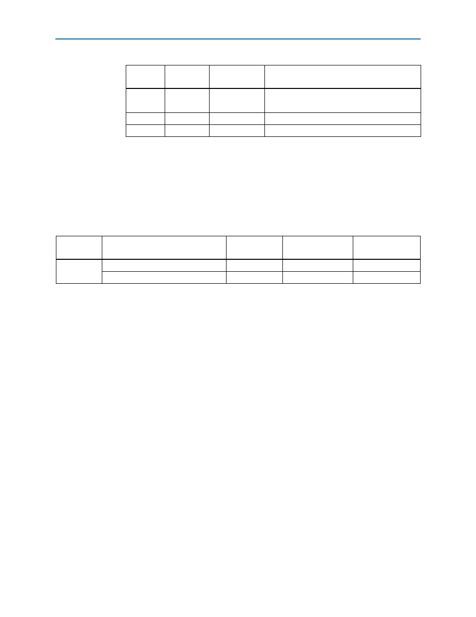
Table 2–32. LCD Pin Definitions and Functions (Part 2 of 2)
Pin
Number
Symbol
Level
Function
Table 2–33. LCD Component References and Manufacturing Information
Board
Reference
Description
Manufacturer
Manufacturer
Part Number
Manufacturer
Website
J3
2×7 pin, 100 mil, vertical header
Samtec
TSM-107-01-G-DV
2×16 character display, 5×8 dot matrix
Lumex Inc.
LCM-S01602DSR/C
