Figure 2–4. jtag chain – Altera Arria II GX FPGA Development Board User Manual
Page 21
Chapter 2: Board Components
2–13
Configuration, Status, and Setup Elements
February 2011
Altera Corporation
Arria II GX FPGA Development Board Reference Manual
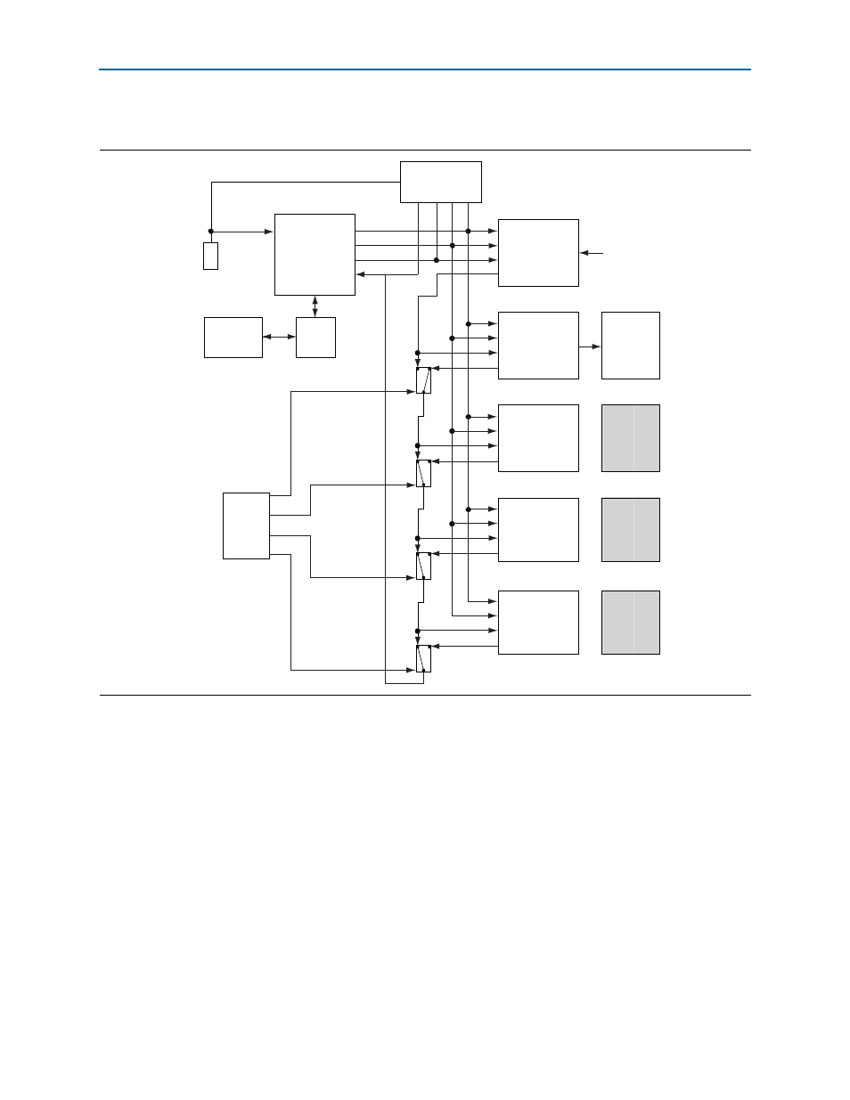
illustrates the JTAG chain.
is located in the JTAG chain header (J9) on the front
of the board. To connect a device or interface in the chain, remove the corresponding
shunt from the jumper. Install a shunt on each of the four jumper positions to only
have the FPGA in the chain.
The MAX
II CPLD EPM2210 System Controller must be in the chain to use some of the
GUI interfaces. For this setting, remove the left-most jumper shunt from the JTAG
chain header (J9).
Flash Memory Programming
Flash memory programming is possible through a variety of methods using the Arria
II GX device.
Figure 2–4. JTAG Chain
Embedded
Blaster
GPIO
TCK
EP2AGX125
FPGA
Analog
Switch
MAX II CPLD
EPM2210
System
Controller
HSMC
Port A
HSMC
Port B
GPIO
TMS
GPIO
TDO
GPIO
TDI
JTAG Master
GPIO
DISABLE
JTAG Master/Slave
JTAG Master/Slave
Installed
HSMC
Card
Installed
HSMC
Card
TCK
TMS
TDI
TDO
TCK
TMS
TDI
TDO
TCK
TMS
TDI
TDO
TCK
TMS
TDI
TDO
JTAG Slave
JTAG Slave
Analog
Switch
Analog
Switch
MAX_JTAG_EN
HSMA_JTAG_EN
HSMB_JTAG_EN
ALWAYS
ENABLED
(in chain)
SW4.6
10-pin
JTAG Connector
Flash
Memory
(on install)
PCI Express
Edge
Connector
JTAG Master/Slave
PCI Express
Motherboard
TCK
TMS
TDI
TDO
Analog
Switch
PCIE_JTAG_EN
USB Type-B
Connector
USB
PHY
J6
J5
JTAG
Chain Header
2x4 Jumper
J9