Altera Arria II GX FPGA Development Board User Manual
Page 52
2–44
Chapter 2: Board Components
Memory
Arria II GX FPGA Development Board Reference Manual
February 2011
Altera Corporation
J7.64
Data bus byte lane 3
DDR2_DQ29
1.8-V SSTL Class I
AN19
J7.74
Data bus byte lane 3
DDR2_DQ30
AK18
J7.76
Data bus byte lane 3
DDR2_DQ31
AF18
J7.67
Write mask byte lane 3
DDR2_DM3
AP20
J7.70
Data strobe P byte lane 3
DDR2_DQS3
AL18
J7.68
Data strobe N byte lane 3
DDR2_DQSN3
AM18
J7.123
Data bus byte lane 4
DDR2_DQ32
AP15
J7.125
Data bus byte lane 4
DDR2_DQ33
AN15
J7.135
Data bus byte lane 4
DDR2_DQ34
AH17
J7.137
Data bus byte lane 4
DDR2_DQ35
AF17
J7.124
Data bus byte lane 4
DDR2_DQ36
AC18
J7.126
Data bus byte lane 4
DDR2_DQ37
AE17
J7.134
Data bus byte lane 4
DDR2_DQ38
AP14
J7.136
Data bus byte lane 4
DDR2_DQ39
AN13
J7.130
Write mask byte lane 4
DDR2_DM4
AH18
J7.131
Data strobe P byte lane 4
DDR2_DQS4
AM16
J7.129
Data strobe N byte lane 4
DDR2_DQSN4
AM17
J7.141
Data bus byte lane 5
DDR2_DQ40
AH16
J7.143
Data bus byte lane 5
DDR2_DQ41
AH15
J7.151
Data bus byte lane 5
DDR2_DQ42
AP10
J7.153
Data bus byte lane 5
DDR2_DQ43
AP9
J7.140
Data bus byte lane 5
DDR2_DQ44
AL16
J7.142
Data bus byte lane 5
DDR2_DQ45
AK16
J7.152
Data bus byte lane 5
DDR2_DQ46
AP12
J7.154
Data bus byte lane 5
DDR2_DQ47
AN12
J7.147
Write mask byte lane 5
DDR2_DM5
AG16
J7.148
Data strobe P byte lane 5
DDR2_DQS5
AK15
J7.146
Data strobe N byte lane 5
DDR2_DQSN5
AL15
J7.157
Data bus byte lane 6
DDR2_DQ48
AN7
J7.159
Data bus byte lane 6
DDR2_DQ49
AP7
J7.173
Data bus byte lane 6
DDR2_DQ50
AP6
J7.175
Data bus byte lane 6
DDR2_DQ51
AP5
J7.158
Data bus byte lane 6
DDR2_DQ52
AF16
J7.160
Data bus byte lane 6
DDR2_DQ53
AL14
J7.174
Data bus byte lane 6
DDR2_DQ54
AE16
J7.176
Data bus byte lane 6
DDR2_DQ55
AL11
J7.170
Write mask byte lane 6
DDR2_DM6
AC15
J7.169
Data strobe P byte lane 6
DDR2_DQS6
AK13
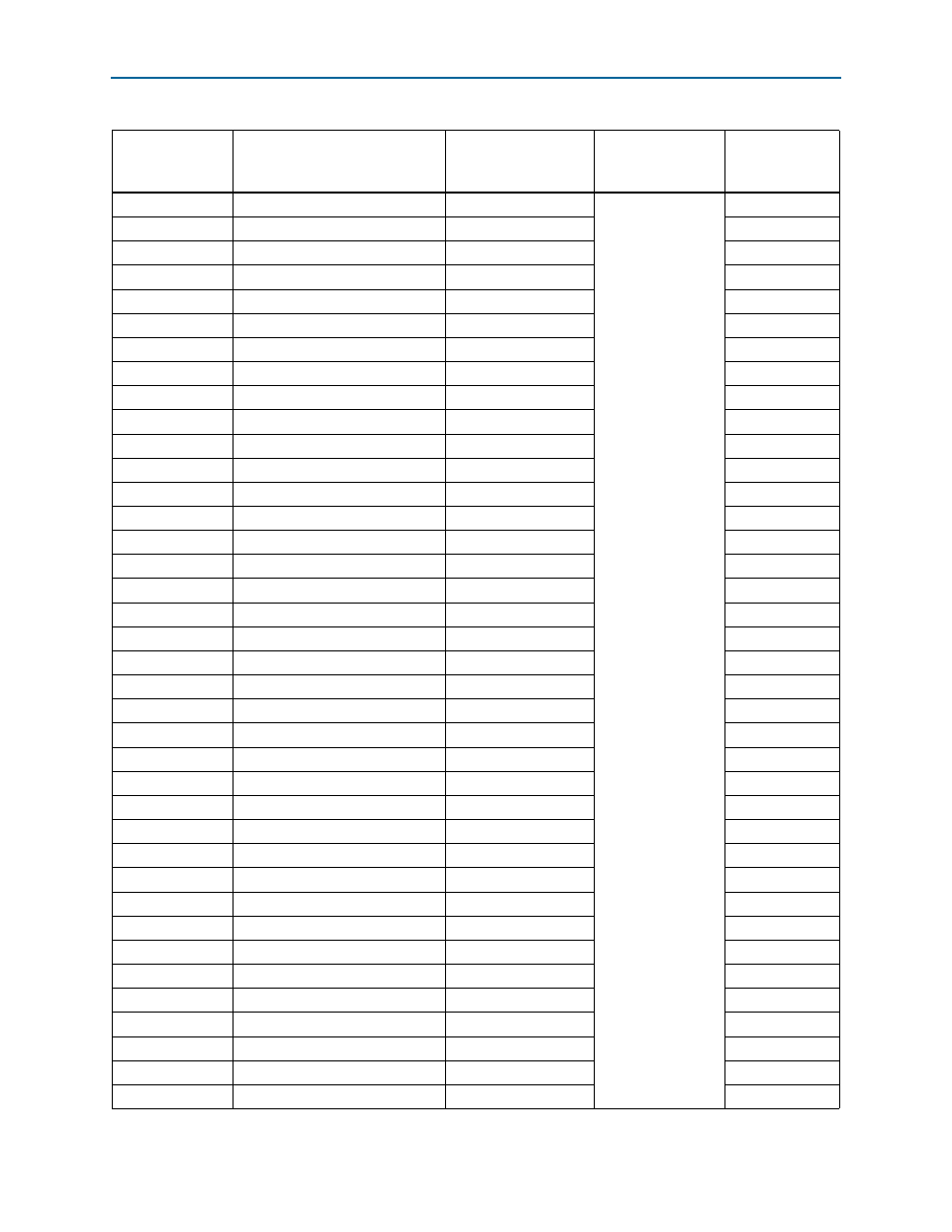
Table 2–42. DDR2 SODIMM Pin Assignments, Signal Names and Functions (Part 3 of 4)
Board Reference
Description
Schematic Signal
Name
I/O Standard
Arria II GX
Device
Pin Number