A. programming the flash memory device, Cfi flash memory map, Appendix a. programming the flash memory device – Altera Stratix V Advanced Systems User Manual
Page 37
February 2013
Altera Corporation
Stratix V Advanced Systems Development Kit
User Guide
A. Programming the Flash Memory
Device
As you develop your own project using the Altera tools, you can program the flash
memory device so that your own design loads from flash memory into the FPGA on
power up. This appendix describes the preprogrammed contents of the common flash
interface (CFI) flash memory device on the Stratix V GX advanced systems board and
how to reprogram the user portions of the flash memory device.
The Stratix V GX advanced systems board ships with the CFI flash device
preprogrammed with a default factory FPGA configuration for running the Board
Test System demonstration.
f
For more information about Altera development tools, refer to the
page of the Altera website.
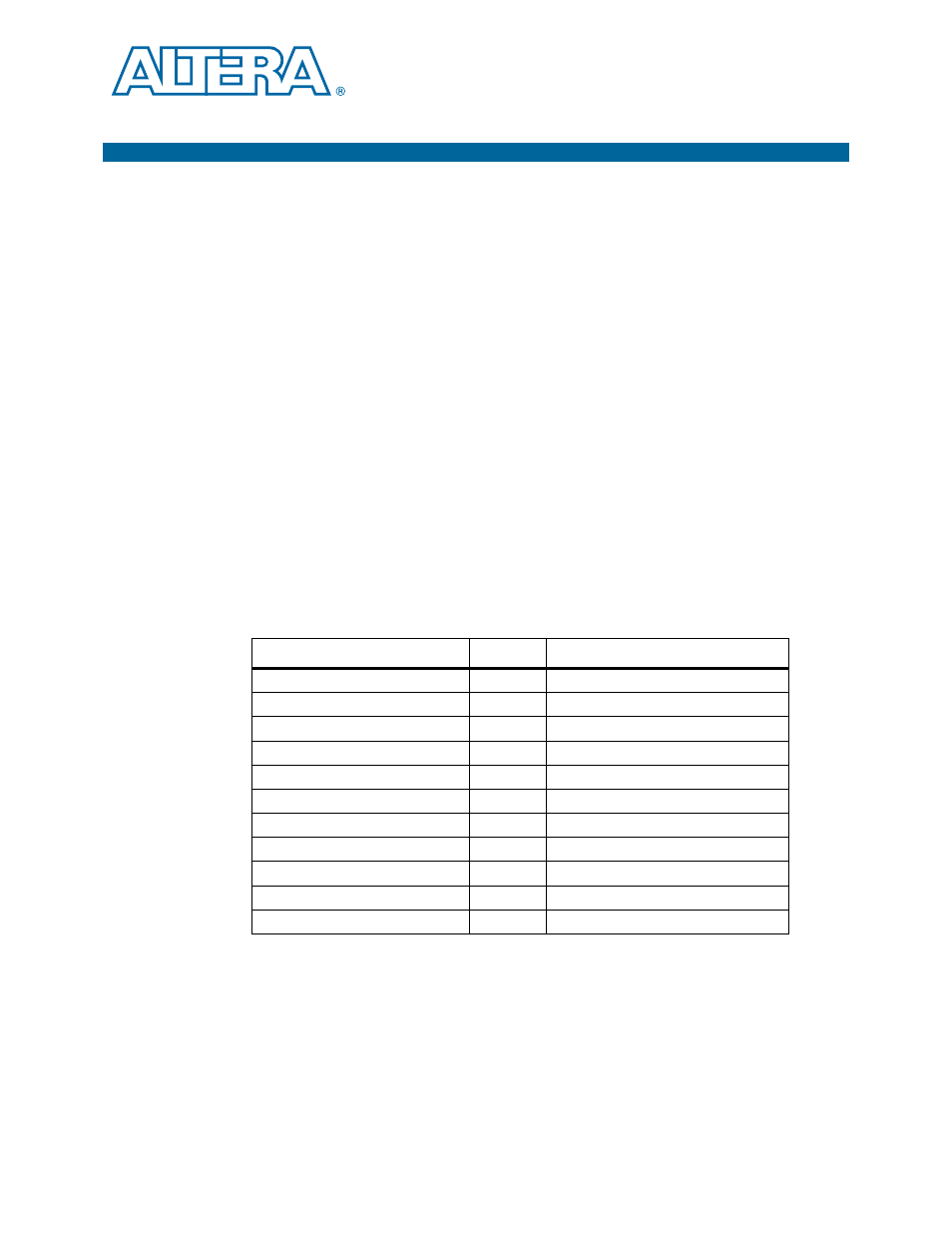
CFI Flash Memory Map
shows the default memory contents of the 1-Gb CFI flash devices. The flash
device has a 16-bit data bus connected to the Max V System Controller that is used to
configure FPGA1 or FPGA2 using FPP x8.
For the FPP to function correctly, the memory map PFL option bits should not be
altered.
c
Altera recommends that you do not overwrite the factory hardware and factory
software images unless you are an expert with the Altera tools.
Table A–1. Byte Address Flash Memory Map
Block Description
Size (KB)
Address Range
Unused
128
0x07FE.0000 - 0x07FF.FFFF
User software
24,320
0x0716.0000 - 0x07F7.FFFF
Factory software
8,192
0x0696.0000 - 0x0715.FFFF
zipfs (html, web content)
8,192
0x0616.0000 - 0x0695.FFFF
Unused
33,152
0x0410.0000 - 0x0615.FFFF
FPGA2 Hardware
33,152
0x020A.0000 - 0x040F.FFFF
FPGA1 Hardware
33,152
0x0002.0000 - 0x0209.FFFF
PFL option bits
32
0x0001.8000 - 0x0001.FFFF
Board information
32
0x0001.0000 - 0x0001.7FFF
Ethernet option bits
32
0x0000.8000 - 0x0000.FFFF
User design reset vector
32
0x0000.0000 - 0x0000.7FFF