Altera Stratix V Advanced Systems User Manual
Page 17
Chapter 4: Development Board Setup
4–5
Factory Default Switch and Jumper Settings
February 2013
Altera Corporation
Stratix V Advanced Systems Development Kit
User Guide
f
For details on the JTAG chain, refer to the
5. Set DIP switch (SW8) to match
6. Set jumper blocks (J2, J3, and J12) to match
.
f
For more information about the FPGA board settings, refer to the
.
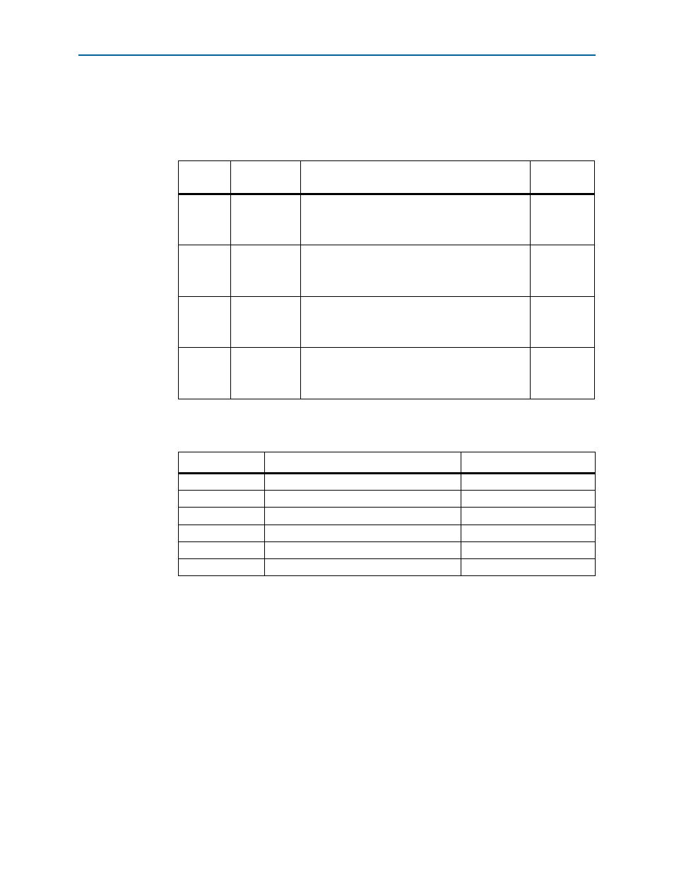
Table 4–5. SW8 PCIe DIP Switch Settings
Switch
Board Label
Function
Default
Position
1
X1
Switch 1 has the following options:
■
When on, x1 presence detect is available.
■
When off, x1 presence detect is unavailable.
Off
2
X4
Switch 2 has the following options:
■
When on, x4 presence detect is available.
■
When off, x4 presence detect is unavailable.
Off
3
X8
Switch 3 has the following options:
■
When on, x8 presence detect is available.
■
When off, x8 presence detect is unavailable.
Off
4
X16
Switch 4 has the following options:
■
When on, x16 presence detect is available.
■
When off, x16 presence detect is unavailable.
Off
Table 4–6. Jumper Settings
Board Reference
Description
Shunt Position
J2
Fan 1 — 5 V and GND power
Fan 1 power connected
J3
VCCIO_FMC 1.8 V
Pins 1-2
J3
VCCIO_FMC 1.5 V
Pins 3-4
J3
VCCIO_FMC 1.2 V
Pins 5-6
J3
VCCIO_FMC 2.5 V
Not installed (Default)
J12
Fan 2 — 5 V and GND power
Fan 2 power connected