Figure 4–2 – Altera Stratix V Advanced Systems User Manual
Page 15
Chapter 4: Development Board Setup
4–3
Factory Default Switch and Jumper Settings
February 2013
Altera Corporation
Stratix V Advanced Systems Development Kit
User Guide
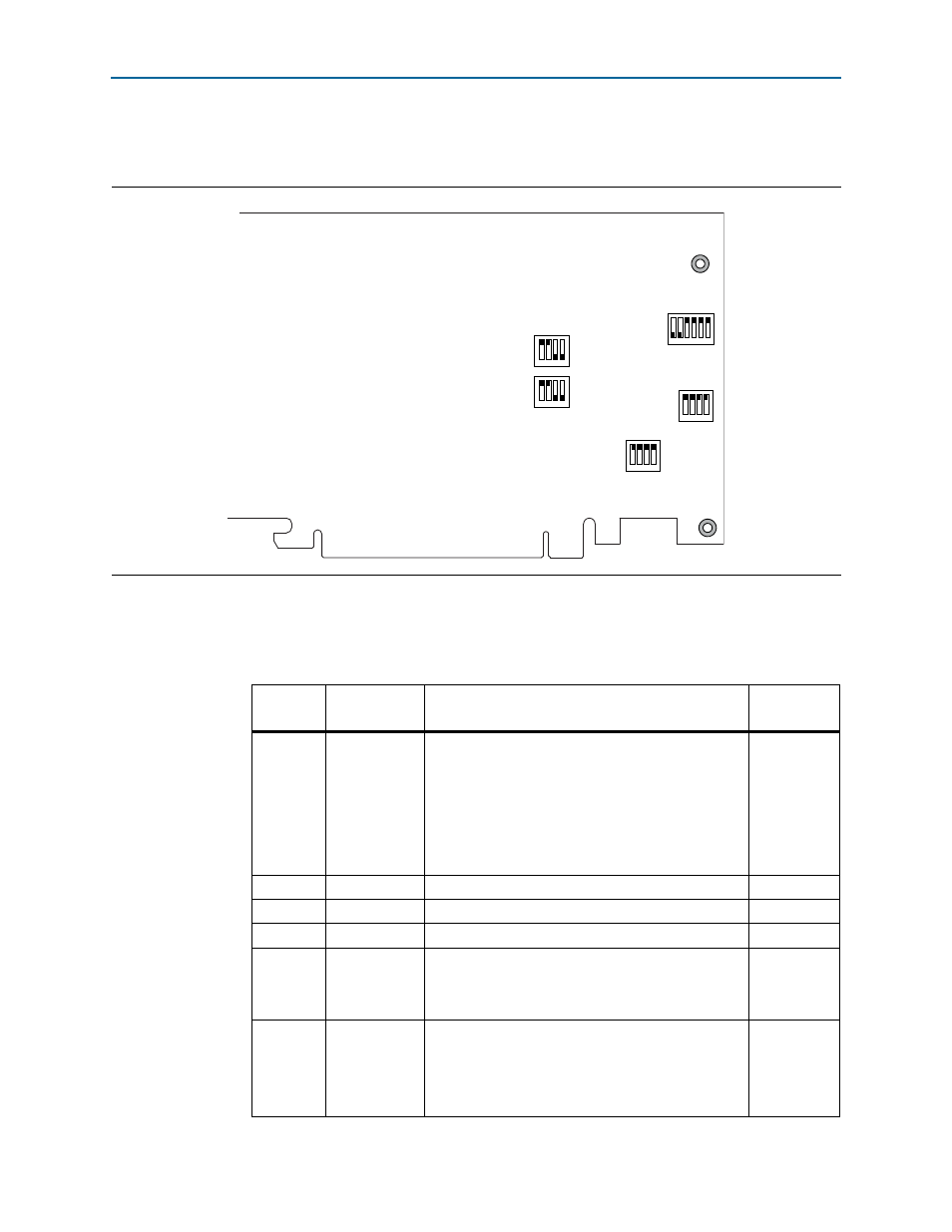
shows the switch locations and the default position of each switch on the
bottom side of the board.
To restore the switches to their factory default settings, perform the following steps:
1. Set DIP switch (SW4) to match
Figure 4–2. Default Settings on the Board Bottom (Detail)
SW6
FPGA2
MSEL
1 2 3 4
1
0
SW5
FPGA1
MSEL
1 2 3 4
1
SW8
1 2 3 4
X1 X4 X8 X16
SW7
1 2 3 4
0
0
1
0
1
SW4
1 2 3 4 5 6
FPGA1_FPP FPGA2_FPP EXTRA0 EXTRA1 CLK_EN CLK_SEL
HSMC JTAG FMC
Table 4–1. SW4 DIP Switch Settings
Switch
Board Label
Function
Default
Position
1
FPGA1_FPP
Switch 1 has the following options:
■
When on (0), FPP x8 is enabled to configure
FPGA1 from flash location 0 and FPGA2 from flash
location 1. FPGA1 MSEL (SW5) pins and FPGA2
MSEL (SW6) pins must be set correctly.
■
When off (1), no design is configured to FPGA1 or
FPGA2 using FPP x8.
On
2
FPGA2_FPP
—
On
3
EXTRA0
—
Off
4
EXTRA1
—
Off
5
CLK_EN
Switch 5 has the following options:
■
When on (0), the on-board oscillator is disabled.
■
When off (1), the on-board oscillator is enabled.
Off
6
CLK_SEL
Switch 6 has the following options:
■
When on (0), the SMA input clock is selected.
■
When off (1), the programmable oscillator clock is
selected.
On