Altera Stratix IV E FPGA User Manual
Page 20
4–4
Chapter 4: Development Board Setup
Factory Default Switch Settings
Stratix IV E FPGA Development Kit User Guide
June 2011
Altera Corporation
3. Set DIP switch bank (SW2) to match
3
CLK100_EN
Switch 3 has the following options:
■
When on, the 100 MHz clock is disabled.
■
When off, the 100 MHz clock is enabled.
Off
4
CLK125_EN
Switch 4 has the following options:
■
When on, the 125 MHz clock is disabled.
■
When off, the 125 MHz clock is enabled.
Off
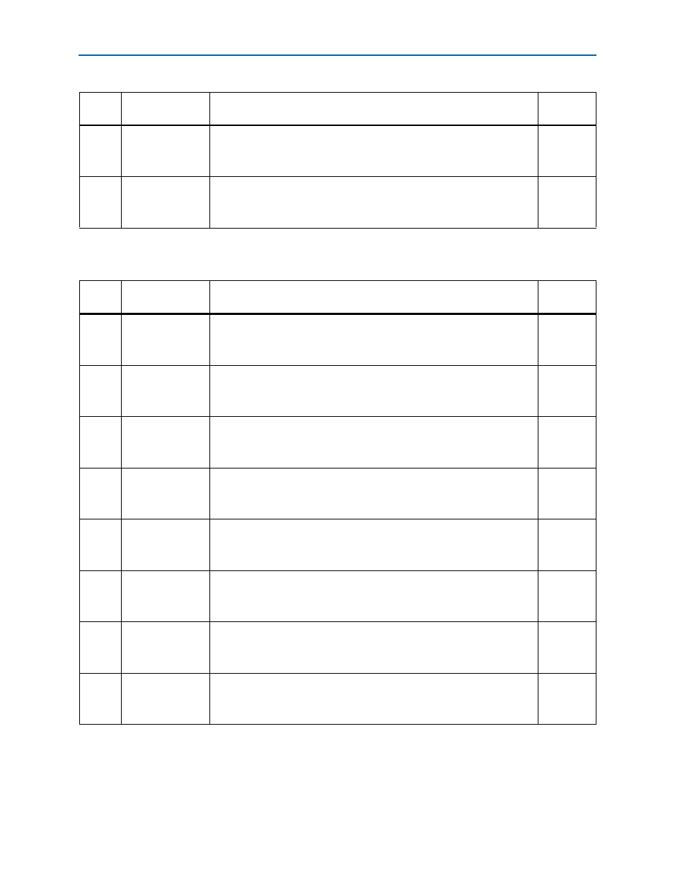
Table 4–1. SW1 Dip Switch Settings (Part 2 of 2)
Switch
Board
Label
Function
Default
Position
Table 4–2. SW2 Dip Switch Settings
Switch
Board
Label
Function
Default
Position
1
DIP0
Switch 1 is a MAX II user-defined switch and has the following options:
■
When closed, a logic 0 is selected.
■
When open, a logic 1 is selected.
Closed
2
DIP1
Switch 2 is a MAX II user-defined switch and has the following options:
■
When closed, a logic 0 is selected.
■
When open, a logic 1 is selected.
Closed
3
DIP2
Switch 3 is a MAX II user-defined switch and has the following options:
■
When closed, a logic 0 is selected.
■
When open, a logic 1 is selected.
Closed
4
DIP3
Switch 4 is a MAX II user-defined switch and has the following options:
■
When closed, a logic 0 is selected.
■
When open, a logic 1 is selected.
Closed
5
DIP4
Switch 5 is a MAX II user-defined switch and has the following options:
■
When closed, a logic 0 is selected.
■
When open, a logic 1 is selected.
Closed
6
DIP5
Switch 6 is a MAX II user-defined switch and has the following options:
■
When closed, a logic 0 is selected.
■
When open, a logic 1 is selected.
Closed
7
DIP6
Switch 7 is a MAX II user-defined switch and has the following options:
■
When closed, a logic 0 is selected.
■
When open, a logic 1 is selected.
Closed
8
CLK66_SEL
Switch 8 has the following options:
■
When closed, the 66 MHz clock is selected.
■
When open, the SMA input clock is selected.
Closed