Max v registers, Max v registers –5 – Altera Cyclone V GT FPGA User Manual
Page 27
Chapter 6: Board Test System
6–5
Using the Board Test System
September 2014
Altera Corporation
Cyclone V GT FPGA Development Kit
User Guide
■
Board P/N
—Indicates the part number of the board.
■
Serial number
—Indicates the serial number of the board.
■
Factory test version
—Indicates the version of the Board Test System currently
running on the board.
■
MAX V ver
—Indicates the version of MAX V code currently running on the
board. The MAX V code resides in the
f
Newer revisions of this code might be available on the
ge of the Altera website.
■
MAC
—Indicates the MAC address of the board.
MAX V Registers
The MAX V registers control allows you to view and change the current MAX V
register values as described in
. Changes to the register values with the GUI
take effect immediately. For example, writing a 0 to SRST resets the board.
■
PSO
—Sets the MAX V PSO register. The following options are available:
■
Use PSR
—Allows the PSR to determine the page of flash memory to use for
FPGA reconfiguration.
■
Use PSS
—Allows the PSS to determine the page of flash memory to use for
FPGA reconfiguration.
■
PSR
—Sets the MAX V PSR register. The numerical values in the list corresponds
to the page of flash memory to load during FPGA reconfiguration. Refer to
for more information.
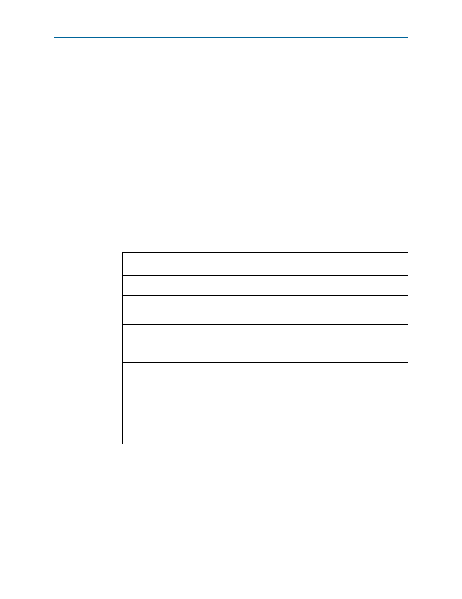
Table 6–1. MAX V Registers
Register Name
Read/Write
Capability
Description
System Reset
(SRST)
Write only
Set to 0 to initiate an FPGA reconfiguration.
Page Select Register
(PSR)
Read / Write
Determines which of the up to three (0-2) pages of flash
memory to use for FPGA reconfiguration. The flash memory
ships with pages 0 and 1 preconfigured.
Page Select Override
(PSO)
Read / Write
When set to 0, the value in PSR determines the page of
flash memory to use for FPGA reconfiguration. When set to
1, the value in PSS determines the page of flash memory to
use for FPGA reconfiguration.
Page Select Switch
(PSS)
Read only
Holds the current value of the illuminated PGM LED (D2-D4)
based on the following encoding:
■
0 = PGM LED (D14) and corresponds to the flash
memory page for the factory hardware design
■
1 = PGM LED (D13) and corresponds to the flash
memory page for the user hardware 1 design
■
2 = PGM LED (D12) and corresponds to the flash
memory page for the user hardware 2 design