Altera Audio Video Development Kit, Stratix IV GX Edition User Manual
Page 30

6–8
Chapter 6: Board Test System
Using the Board Test System
Audio Video Development Kit, Stratix IV GX Edition User Guide
© November 2009 Altera
Corporation
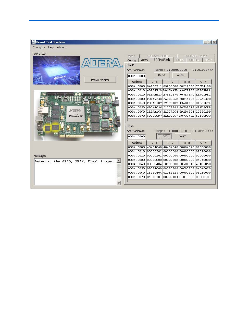
The following sections describe the controls on the SRAM&Flash tab.
SRAM
The SRAM control allows you to read and write the SRAM on your board. Type a
starting address in the text box and click Read. Values starting at the specified address
appear in the table. The SRAM addresses display in the format the Nios II processor
within the FPGA uses, that is, each SRAM address is offset by 0x00400000. Thus, the
first location in SRAM appears as 0x00400000 in the GUI.
1
If you enter an address outside of the 0x00400000 to 0x005FFFFF SRAM address
space, a warning message identifies the valid SRAM address range.
To update the SRAM contents, change values in the table and click Write. The
application writes the new values to SRAM and then reads the values back to
guarantee that the graphical display accurately reflects the memory contents.
Figure 6–4. The SRAM&Flash Tab
- MAX 10 JTAG (15 pages)
- MAX 10 Power (21 pages)
- Unique Chip ID (12 pages)
- Remote Update IP Core (43 pages)
- Device-Specific Power Delivery Network (28 pages)
- Device-Specific Power Delivery Network (32 pages)
- Hybrid Memory Cube Controller (69 pages)
- ALTDQ_DQS IP (117 pages)
- MAX 10 Embedded Memory (71 pages)
- MAX 10 Embedded Multipliers (37 pages)
- MAX 10 Clocking and PLL (86 pages)
- MAX 10 FPGA (26 pages)
- MAX 10 FPGA (56 pages)
- USB-Blaster II (22 pages)
- GPIO (22 pages)
- LVDS SERDES (27 pages)
- User Flash Memory (33 pages)
- ALTDQ_DQS2 (100 pages)
- Avalon Tri-State Conduit Components (18 pages)
- Cyclone V Avalon-MM (166 pages)
- Cyclone III FPGA Starter Kit (36 pages)
- Cyclone V Avalon-ST (248 pages)
- Stratix V Avalon-ST (286 pages)
- Stratix V Avalon-ST (293 pages)
- DDR3 SDRAM High-Performance Controller and ALTMEMPHY IP (10 pages)
- Arria 10 Avalon-ST (275 pages)
- Avalon Verification IP Suite (224 pages)
- Avalon Verification IP Suite (178 pages)
- FFT MegaCore Function (50 pages)
- DDR2 SDRAM High-Performance Controllers and ALTMEMPHY IP (140 pages)
- Floating-Point (157 pages)
- Integer Arithmetic IP (157 pages)
- Embedded Peripherals IP (336 pages)
- JESD204B IP (158 pages)
- Low Latency Ethernet 10G MAC (109 pages)
- LVDS SERDES Transmitter / Receiver (72 pages)
- Nios II Embedded Evaluation Kit Cyclone III Edition (3 pages)
- Nios II Embedded Evaluation Kit Cyclone III Edition (80 pages)
- IP Compiler for PCI Express (372 pages)
- Parallel Flash Loader IP (57 pages)
- Nios II C2H Compiler (138 pages)
- RAM-Based Shift Register (26 pages)
- RAM Initializer (36 pages)
- Phase-Locked Loop Reconfiguration IP Core (51 pages)
- DCFIFO (28 pages)
